SLPS667B February 2017 – June 2024 CSD17318Q2
PRODUCTION DATA
- 1
- 1Features
- 2Applications
- 3Description
- 4Specifications
- 5Device and Documentation Support
- 6Revision History
- 7Mechanical, Packaging, and Orderable Information
Package Options
Refer to the PDF data sheet for device specific package drawings
Mechanical Data (Package|Pins)
- DQK|6
Thermal pad, mechanical data (Package|Pins)
Orderable Information
3 Description
This 30V, 12.6mΩ, 2mm × 2mm SON NexFET™ power MOSFET is designed to minimize losses in power conversion applications and optimized for 5V gate drive applications. The 2mm × 2mm SON offers excellent thermal performance for the size of the package.
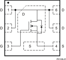
 Figure 3-1 Top View
Product Summary
| TA = 25°C | TYPICAL VALUE | UNIT | ||
|---|---|---|---|---|
| VDS | Drain-to-Source Voltage | 30 | V | |
| Qg | Gate Charge Total (4.5V) | 6.0 | nC | |
| Qgd | Gate Charge Gate-to-Drain | 1.3 | nC | |
| RDS(on) | Drain-to-Source On-Resistance | VGS = 2.5V | 20 | mΩ |
| VGS = 4.5V | 13.9 | |||
| VGS = 8V | 12.6 | |||
| VGS(th) | Threshold Voltage | 0.9 | V | |
Device Information(1)
| PART NUMBER | QTY | MEDIA | PACKAGE | SHIP |
|---|---|---|---|---|
| CSD17318Q2 | 3000 | 7 Inch Reel | SON 2.00mm × 2.00mm Plastic Package | Tape and Reel |
| CSD17318Q2T | 250 |
(1) For all available packages, see the orderable addendum at the end of the data sheet.
Absolute Maximum Ratings
| TA = 25°C | VALUE | UNIT | |
|---|---|---|---|
| VDS | Drain-to-Source Voltage | 30 | V |
| VGS | Gate-to-Source Voltage | ±10 | V |
| ID | Continuous Drain Current (Package Limited) | 21.5 | A |
| Continuous Drain Current (Silicon Limited), TC = 25°C | 25 | ||
| Continuous Drain Current(1) | 10 | ||
| IDM | Pulsed Drain Current, TA = 25°C(2) | 68 | A |
| PD | Power Dissipation(1) | 2.5 | W |
| Power Dissipation, TC = 25°C | 16 | ||
| TJ, TSTG | Operating Junction, Storage Temperature | –55 to 150 | °C |
| EAS | Avalanche Energy, Single
Pulse, ID = 12.4A, L = 0.1mH, RG = 25Ω | 7.7 | mJ |
(1) Typical RθJA = 55°C/W on a 1in2, 2oz Cu pad on a
0.06in thick FR4 PCB.
0.06in thick FR4 PCB.
(2) Max RθJC = 7°C/W, pulse duration ≤ 100μs, duty cycle ≤ 1%.
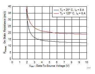
 On-State
Resistance vs Gate to Source Voltage
 |
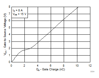
 Gate
Charge
 |