SLPS574B February 2016 – April 2018 CSD87335Q3D
PRODUCTION DATA.
- 1Features
- 2Applications
- 3Description
- 4Revision History
- 5Specifications
- 6Applications and Implementation
- 7Recommended PCB Design Overview
- 8Device and Documentation Support
- 9Mechanical, Packaging, and Orderable Information
Package Options
Mechanical Data (Package|Pins)
- DQZ|8
Thermal pad, mechanical data (Package|Pins)
Orderable Information
6.5.3 Calculating SOA Adjustments
- SOA adjustment for input voltage ≈ 0.14°C (Figure 6)
- SOA adjustment for output voltage ≈ 0.17°C (Figure 7)
- SOA adjustment for switching frequency ≈ 1.32°C (Figure 5)
- SOA adjustment for output inductor ≈ 0.18°C (Figure 8)
- Final calculated SOA adjustment = 0.14 + 0.17 + 1.32 + 0.18 ≈ 1.81°C
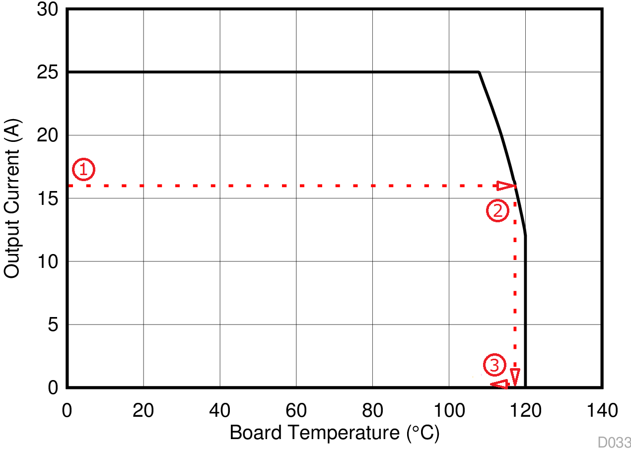
In the design example above, the estimated power loss of the CSD87335Q3D would increase to 2.14 W. In addition, the maximum allowable board and/or ambient temperature would have to decrease by 1.81°C. Figure 32 graphically shows how the SOA curve would be adjusted accordingly.
- Start by drawing a horizontal line from the application current to the SOA curve.
- Draw a vertical line from the SOA curve intercept down to the board/ambient temperature.
- Adjust the SOA board/ambient temperature by subtracting the temperature adjustment value.
In the design example, the SOA temperature adjustment yields a reduction in allowable board/ambient temperature of 1.81°C. In the event the adjustment value is a negative number, subtracting the negative number would yield an increase in allowable board/ambient temperature.
 Figure 32. Power Block SOA