-
CSD95378BQ5M Synchronous Buck NexFET Smart Power Stage
Package Options
Refer to the PDF data sheet for device specific package drawings
Mechanical Data (Package|Pins)
- DQP|12
Thermal pad, mechanical data (Package|Pins)
Orderable Information
CSD95378BQ5M Synchronous Buck NexFET Smart Power Stage
1 Features
- 60-A Continuous Operating Current Capability
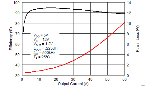
- 93.4% System Efficiency at 30 A
- Low-Power Loss of 2.8 W at 30 A
- High-Frequency Operation (up to 1.25 MHz)
- Diode Emulation Mode With FCCM
- Temperature Compensated Bi-Directional Current Sense
- Analog Temperature Output (400 mV at 0°C)
- Fault Monitoring
- High-Side Short, Overcurrent, and Overtemperature Protection
- 3.3-V and 5-V PWM Signal Compatible
- Tri-State PWM Input
- Integrated Bootstrap Diode
- Optimized Dead Time for Shoot-Through Protection
- High-Density SON 5-mm × 6-mm Footprint
- Ultra-Low-Inductance Package
- System Optimized PCB Footprint
- RoHS Compliant – Lead-Free Terminal Plating
- Halogen Free
2 Applications
- Multiphase Synchronous Buck Converters
- High-Frequency Applications
- High-Current, Low-Duty-Cycle Applications
- POL DC-DC Converters
- Memory and Graphic Cards
- Desktop and Server VR11.x / VR12.x V-core and Memory Synchronous Converters
3 Description
The CSD95378BQ5M NexFET™ smart power stage is a highly optimized design for use in a high-power, high-density synchronous buck converter. This product integrates the driver IC and power MOSFETs to complete the power stage switching function. This combination produces high-current, high-efficiency, and high speed switching capability in a small
5-mm × 6-mm outline package. It also integrates the accurate current sensing and temperature sensing functionality to simplify system design and improve accuracy. In addition, the PCB footprint is optimized to help reduce design time and simplify the completion of the overall system design.
Device Information(1)
| DEVICE | MEDIA | QTY | PACKAGE | SHIP |
|---|---|---|---|---|
| CSD95378BQ5M | 13-Inch Reel | 2500 | SON 5.00-mm × 6.00-mm Package |
Tape and Reel |
| CSD95378BQ5MT | 7-Inch Reel | 250 |
- For all available packages, see the orderable addendum at the end of the data sheet.
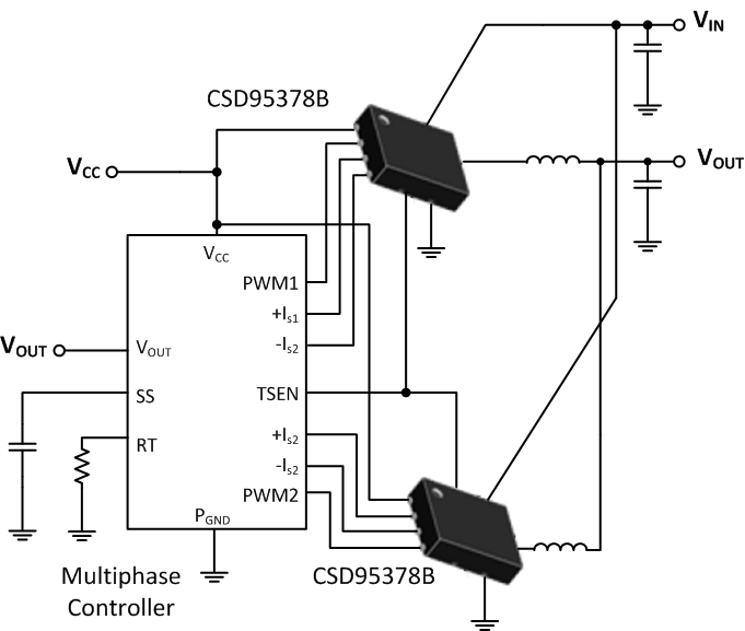
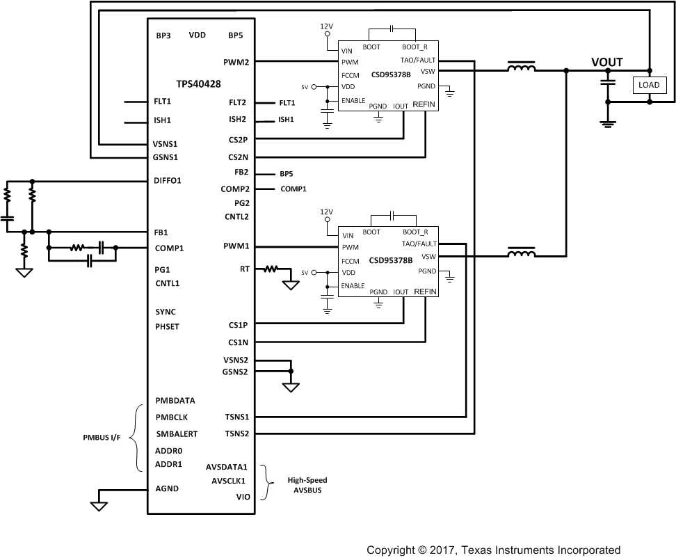
Application Diagram

Typical Power Stage Efficiency and Power Loss

4 Revision History
Changes from A Revision (July 2014) to B Revision
- Updated the CSD95378B parts in the Application SchematicGo
- Added the Receiving Notification of Documentation Updates and Community Resources sections in Device and Documentation SupportGo
Changes from * Revision (April 2014) to A Revision
- Updated the controller IC in the Application Schematic to the TPS40428Go
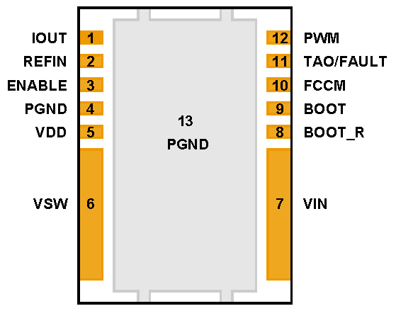
5 Pin Configuration and Functions

Pin Functions
| PIN | DESCRIPTION | |
|---|---|---|
| NAME | NO. | |
| BOOT | 9 | Bootstrap capacitor connection. Connect a minimum of 0.1-µF, 16-V, X7R ceramic capacitor from BOOT to BOOT_R pins. The bootstrap capacitor provides the charge to turn on the control FET. The bootstrap diode is integrated. |
| BOOT_R | 8 | Return path for HS gate driver, connected to VSW internally. |
| ENABLE | 3 | Enables device operation. If ENABLE = logic HIGH, turns on device. If ENABLE = logic LOW, the device is turned off and both MOSFET gates are actively pulled low. An internal 100-kΩ pulldown resistor will pull the ENABLE pin LOW if left floating. |
| FCCM | 10 | This pin enables the Diode Emulation function. When this pin is held LOW, Diode Emulation Mode is enabled for sync FET. When FCCM is HIGH, the device is operated in Forced Continuous Conduction Mode. An internal 5-µA current source will pull the FCCM pin to 3.3 V if left floating. |
| IOUT | 1 | Output of current sensing amplifier. V(IOUT) – V(REFIN) is proportional to the phase current. |
| PGND | 4 | Power ground, connected directly to pin 13. |
| PGND | 13 | Power ground. |
| PWM | 12 | Pulse width modulated tri-state input from external controller. Logic LOW sets control FET gate low and sync FET gate high. Logic HIGH sets control FET gate high and sync FET gate low. Open or Hi-Z sets both MOSFET gates low if greater than the tri-state shutdown hold-off time (t3HT). |
| REFIN | 2 | External reference voltage input for current sensing amplifier. |
| TAO/ FAULT |
11 | Temperature analog output. Reports a voltage proportional to the die temperature. An ORing diode is integrated in the IC. When used in multiphase application, a single wire can be used to connect the TAO pins of all the ICs. Only the highest temperature will be reported. TAO will be pulled up to 3.3 V if thermal shutdown occurs. TAO should be bypassed to PGND with a 1-nF, 16-V, X7R ceramic capacitor. |
| VDD | 5 | Supply voltage to gate driver and internal circuitry. |
| VIN | 7 | Input voltage pin. Connect input capacitors close to this pin. |
| VSW | 6 | Phase node connecting the HS MOSFET source and LS MOSFET drain - pin connection to the output inductor. |
6 Specifications
6.1 Absolute Maximum Ratings
TA = 25°C (unless otherwise noted)(1)| MIN | MAX | UNIT | ||
|---|---|---|---|---|
| VIN to PGND | –0.3 | 25 | V | |
| VIN to VSW | –0.3 | 25 | V | |
| VIN to VSW (10 ns) | –7 | 27 | V | |
| VSW to PGND | –0.3 | 20 | V | |
| VSW to PGND (10 ns) | –7 | 23 | V | |
| VDD to PGND | –0.3 | 7 | V | |
| ENABLE, PWM, FCCM. TAO, IOUT, REFIN to PGND | –0.3 | VDD + 0.3 V | V | |
| BOOT to BOOT_R(2) | –0.3 | VDD + 0.3 V | V | |
| Power dissipation, PD | 12 | W | ||
| Operating junction temperature, TJ | –55 | 150 | °C | |
| Storage temperature, Tstg | –55 | 150 | °C | |
6.2 ESD Ratings
| MIN | MAX | UNIT | |||
|---|---|---|---|---|---|
| V(ESD) | Electrostatic discharge | Human-body model (HBM) | –2000 | 2000 | V |
| Charged-device model (CDM) | –500 | 500 | |||
6.3 Recommended Operating Conditions
TA = 25°C (unless otherwise noted)| MIN | MAX | UNIT | |||
|---|---|---|---|---|---|
| VDD | Gate drive voltage | 4.5 | 5.5 | V | |
| VIN | Input supply voltage(1) | 16 | V | ||
| VOUT | Output voltage | 5.5 | V | ||
| IOUT | Continuous output current | VIN = 12 V, VDD = 5 V, VOUT = 1.2 V, ƒSW = 500 kHz, LOUT = 0.225 µH(2) |
60 | ||
| IOUT-PK | Peak output current(3) | 90 | A | ||
| ƒSW | Switching frequency | CBST = 0.1 µF (min) | 1250 | kHz | |
| On-time duty cycle | ƒSW = 1 MHz | 85% | |||
| Minimum PWM on time | 40 | ns | |||
| Operating temperature | –40 | 125 | °C | ||
6.4 Thermal Information
TA = 25°C (unless otherwise noted)| THERMAL METRIC | MIN | TYP | MAX | UNIT | |
|---|---|---|---|---|---|
| RθJC | Junction-to-case (top-of-package) thermal resistance(1) | 15 | °C/W | ||
| RθJB | Junction-to-board thermal resistance(2) | 1.5 | |||
8 Device and Documentation Support
8.1 Receiving Notification of Documentation Updates
To receive notification of documentation updates, navigate to the device product folder on ti.com. In the upper right corner, click on Alert me to register and receive a weekly digest of any product information that has changed. For change details, review the revision history included in any revised document.
8.2 Community Resources
The following links connect to TI community resources. Linked contents are provided "AS IS" by the respective contributors. They do not constitute TI specifications and do not necessarily reflect TI's views; see TI's Terms of Use.
-
TI E2E™ Online Community TI's Engineer-to-Engineer (E2E) Community. Created to foster collaboration among engineers. At e2e.ti.com, you can ask questions, share knowledge, explore ideas and help solve problems with fellow engineers.
-
Design Support TI's Design Support Quickly find helpful E2E forums along with design support tools and contact information for technical support.
8.3 Trademarks
NexFET, E2E are trademarks of Texas Instruments.
8.4 Electrostatic Discharge Caution

These devices have limited built-in ESD protection. The leads should be shorted together or the device placed in conductive foam during storage or handling to prevent electrostatic damage to the MOS gates.
8.5 Glossary
SLYZ022 — TI Glossary.
This glossary lists and explains terms, acronyms, and definitions.
9 Mechanical, Packaging, and Orderable Information
The following pages include mechanical packaging and orderable information. This information is the most current data available for the designated devices. This data is subject to change without notice and revision of this document. For browser-based versions of this data sheet, refer to the left-hand navigation.
9.1 Mechanical Drawing

| DIM | MILLIMETERS | INCHES | ||||
|---|---|---|---|---|---|---|
| MIN | NOM | MAX | MIN | NOM | MAX | |
| A | 1.400 | 1.450 | 1.500 | 0.057 | 0.059 | 0.061 |
| a1 | 0.000 | 0.000 | 0.050 | 0.000 | 0.000 | 0.002 |
| b | 0.200 | 0.250 | 0.320 | 0.008 | 0.010 | 0.013 |
| b1 | 2.750 TYP | 0.108 TYP | ||||
| b2 | 0.200 | 0.250 | 0.320 | 0.008 | 0.010 | 0.013 |
| b3 | 0.250 TYP | 0.010 TYP | ||||
| c1 | 0.150 | 0.200 | 0.250 | 0.006 | 0.008 | 0.010 |
| c2 | 0.200 | 0.250 | 0.300 | 0.008 | 0.010 | 0.012 |
| D2 | 5.300 | 5.400 | 5.500 | 0.209 | 0.213 | 0.217 |
| d | 0.200 | 0.250 | 0.300 | 0.008 | 0.010 | 0.012 |
| d1 | 0.350 | 0.400 | 0.450 | 0.014 | 0.016 | 0.018 |
| d2 | 1.900 | 2.000 | 2.100 | 0.075 | 0.079 | 0.083 |
| E | 5.900 | 6.000 | 6.100 | 0.232 | 0.236 | 0.240 |
| E1 | 4.900 | 5.000 | 5.100 | 0.193 | 0.197 | 0.201 |
| E2 | 3.200 | 3.300 | 3.400 | 0.126 | 0.130 | 0.134 |
| e | 0.500 TYP | 0.020 TYP | ||||
| K | 0.350 TYP | 0.014 TYP | ||||
| L | 0.400 | 0.500 | 0.600 | 0.016 | 0.020 | 0.024 |
| L1 | 0.210 | 0.310 | 0.410 | 0.008 | 0.012 | 0.016 |
| θ | 0.00 | — | — | 0.00 | — | — |
9.2 Recommended PCB Land Pattern

- Dimensions are in mm (in).
9.3 Recommended Stencil Opening

- Dimensions are in mm (in).
- Stencil thickness is 100 µm.
IMPORTANT NOTICE
Texas Instruments Incorporated (TI) reserves the right to make corrections, enhancements, improvements and other changes to its semiconductor products and services per JESD46, latest issue, and to discontinue any product or service per JESD48, latest issue. Buyers should obtain the latest relevant information before placing orders and should verify that such information is current and complete.
TI’s published terms of sale for semiconductor products (http://www.ti.com/sc/docs/stdterms.htm) apply to the sale of packaged integrated circuit products that TI has qualified and released to market. Additional terms may apply to the use or sale of other types of TI products and services.
Reproduction of significant portions of TI information in TI data sheets is permissible only if reproduction is without alteration and is accompanied by all associated warranties, conditions, limitations, and notices. TI is not responsible or liable for such reproduced documentation. Information of third parties may be subject to additional restrictions. Resale of TI products or services with statements different from or beyond the parameters stated by TI for that product or service voids all express and any implied warranties for the associated TI product or service and is an unfair and deceptive business practice. TI is not responsible or liable for any such statements.
Buyers and others who are developing systems that incorporate TI products (collectively, “Designers”) understand and agrees that Designers remain responsible for using their independent analysis, evaluation and judgment in designing their systems and products, and have full and exclusive responsibility to assure the safety of their products and compliance of their products (and of all TI products used in or for such Designers’ products) with all applicable regulations, laws and other applicable requirements. Designers represent that, with respect to their applications, they have all the necessary expertise to create and implement safeguards that (1) anticipate dangerous consequences of failures, (2) monitor failures and their consequences, and (3) lessen the likelihood of failures that might cause harm and take appropriate actions. Designers agree that prior to using or distributing any systems that include TI products, they will thoroughly test such systems and the functionality of such TI products as used in such systems.
TI’s provision of reference designs and any other technical, applications or design advice, quality characterization, reliability data or other information or services does not expand or otherwise alter TI’s applicable published warranties or warranty disclaimers for TI products, and no additional obligations or liabilities arise from TI providing such reference designs or other items.
Designers are authorized to use, copy and modify any individual TI reference design only in connection with the development of end products that include the TI product(s) identified in that reference design. HOWEVER, NO OTHER LICENSE, EXPRESS OR IMPLIED, BY ESTOPPEL OR OTHERWISE TO ANY OTHER TI INTELLECTUAL PROPERTY RIGHT, AND NO LICENSE TO ANY TECHNOLOGY OR INTELLECTUAL PROPERTY RIGHT OF TI OR ANY THIRD PARTY IS GRANTED HEREIN, including but not limited to any patent right, copyright, mask work right, or other intellectual property right relating to any combination, machine, or process in which TI products or services are used. Information published by TI regarding third-party products or services does not constitute a license to use such products or services, or a warranty or endorsement thereof. Use of the reference design or other items described above may require a license from a third party under the patents or other intellectual property of the third party, or a license from TI under the patents or other intellectual property of TI.
TI REFERENCE DESIGNS AND OTHER ITEMS DESCRIBED ABOVE ARE PROVIDED “AS IS” AND WITH ALL FAULTS. TI DISCLAIMS ALL OTHER WARRANTIES OR REPRESENTATIONS, EXPRESS OR IMPLIED, REGARDING THE REFERENCE DESIGNS OR USE OF THE REFERENCE DESIGNS, INCLUDING BUT NOT LIMITED TO ACCURACY OR COMPLETENESS, TITLE, ANY EPIDEMIC FAILURE WARRANTY AND ANY IMPLIED WARRANTIES OF MERCHANTABILITY, FITNESS FOR A PARTICULAR PURPOSE, AND NON-INFRINGEMENT OF ANY THIRD PARTY INTELLECTUAL PROPERTY RIGHTS.
TI SHALL NOT BE LIABLE FOR AND SHALL NOT DEFEND OR INDEMNIFY DESIGNERS AGAINST ANY CLAIM, INCLUDING BUT NOT LIMITED TO ANY INFRINGEMENT CLAIM THAT RELATES TO OR IS BASED ON ANY COMBINATION OF PRODUCTS AS DESCRIBED IN A TI REFERENCE DESIGN OR OTHERWISE. IN NO EVENT SHALL TI BE LIABLE FOR ANY ACTUAL, DIRECT, SPECIAL, COLLATERAL, INDIRECT, PUNITIVE, INCIDENTAL, CONSEQUENTIAL OR EXEMPLARY DAMAGES IN CONNECTION WITH OR ARISING OUT OF THE REFERENCE DESIGNS OR USE OF THE REFERENCE DESIGNS, AND REGARDLESS OF WHETHER TI HAS BEEN ADVISED OF THE POSSIBILITY OF SUCH DAMAGES.
Unless TI has explicitly designated an individual product as meeting the requirements of a particular industry standard (e.g., ISO/TS 16949 and ISO 26262), TI is not responsible for any failure to meet such industry standard requirements.
Where TI specifically promotes products as facilitating functional safety or as compliant with industry functional safety standards, such products are intended to help enable customers to design and create their own applications that meet applicable functional safety standards and requirements. Using products in an application does not by itself establish any safety features in the application. Designers must ensure compliance with safety-related requirements and standards applicable to their applications. Designer may not use any TI products in life-critical medical equipment unless authorized officers of the parties have executed a special contract specifically governing such use. Life-critical medical equipment is medical equipment where failure of such equipment would cause serious bodily injury or death (e.g., life support, pacemakers, defibrillators, heart pumps, neurostimulators, and implantables). Such equipment includes, without limitation, all medical devices identified by the U.S. Food and Drug Administration as Class III devices and equivalent classifications outside the U.S.
TI may expressly designate certain products as completing a particular qualification (e.g., Q100, Military Grade, or Enhanced Product). Designers agree that it has the necessary expertise to select the product with the appropriate qualification designation for their applications and that proper product selection is at Designers’ own risk. Designers are solely responsible for compliance with all legal and regulatory requirements in connection with such selection.
Designer will fully indemnify TI and its representatives against any damages, costs, losses, and/or liabilities arising out of Designer’s non-compliance with the terms and provisions of this Notice.
IMPORTANT NOTICE
| Mailing Address: Texas Instruments, Post Office Box 655303, Dallas, Texas 75265 Copyright © 2017, Texas Instruments Incorporated |
