-
DAC121S101QML-SP Radiation Hardened 12-Bit Micro Power Digital-to-Analog Converter With Rail-to-Rail Output
- 1 Features
- 2 Applications
- 3 Description
- 4 Revision History
- 5 Pin Configuration and Functions
-
6 Specifications
- 6.1 Absolute Maximum Ratings
- 6.2 ESD Ratings
- 6.3 Recommended Operating Conditions
- 6.4 Thermal Information
- 6.5 DAC121S101QML-SP Electrical Characteristics DC Parameters
- 6.6 DAC121S101QML-SP Electrical Characteristics AC and Timing Characteristics
- 6.7 DAC121S101QML Electrical Characteristics Radiation Electrical Characteristics
- 6.8 DAC121S101QML-SP Electrical Characteristics Operating Life Test Delta Parameters TA at 25°C
- 6.9 Typical Characteristics
- 7 Detailed Description
- 8 Application and Implementation
- 9 Power Supply Recommendations
- 10Layout
- 11Device and Documentation Support
- 12Mechanical, Packaging, and Orderable Information
- IMPORTANT NOTICE
Package Options
Mechanical Data (Package|Pins)
- NAC|10
- Y|0
Thermal pad, mechanical data (Package|Pins)
Orderable Information
DAC121S101QML-SP Radiation Hardened 12-Bit Micro Power Digital-to-Analog Converter With Rail-to-Rail Output
1 Features
-
5962R07726
- Total Ionizing Dose 100 krad(Si)
- Single Event Latch-up Immune
120 MeV-cm2/mg - Single Event Functional Interrupt Immune
120 MeV-cm2/mg (See Radiation Report)
- Ensured Monotonicity
- Low Power Operation
- Rail-to-Rail Voltage Output
- Power-On Reset to Zero Volts Output
- SYNC Interrupt Facility
- Wide Power Supply Range (2.7 V to 5.5 V)
- Small Packages
- Power-Down Feature
- Key Specifications
- Resolution: 12 Bits
- DNL: +0.21, –0.10 LSB (Typical)
- Output Settling Time: 12.5 µs (Typical)
- Zero Code Error: 2.1 mV (Typical)
- Full-Scale Error: −0.04% FS (Typical)
- Power Dissipation
- Normal Mode: 0.52 mW (3.6 V) and 1.19 mW (5.5 V) Typical
- Power-Down Mode: 0.014 µW (3.6 V) and 0.033 µW (5.5 V) Typical
2 Applications
- Satellites
- Altitude and Orbit Control
- Precision Sensors
- Motor Control
- High Temperatures
3 Description
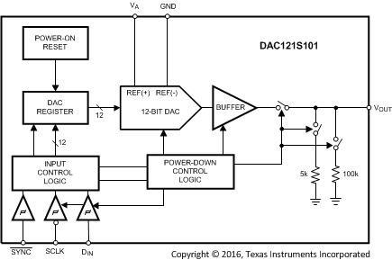
The DAC121S101QML-SP device is a full-featured, general-purpose, 12-bit voltage-output digital-to-analog converter (DAC) that can operate from a single 2.7-V to 5.5-V supply and consumes just
177 µA of current at 3.6 V. The on-chip output amplifier allows rail-to-rail output swing and the three-wire serial interface operates at clock rates up to
20 MHz over the specified supply voltage range and is compatible with standard SPI, QSPI, MICROWIRE, and DSP interfaces.
The supply voltage for the DAC121S101QML-SP serves as its voltage reference, providing the widest possible output dynamic range. A power-on reset circuit ensures that the DAC output powers up to zero volts and remains there until there is a valid write to the device. A power-down feature reduces power consumption to less than a microWatt.
The low power consumption and small packages of the DAC121S101QML-SP make it an excellent choice for use in battery-operated equipment.
Device Information(1)
| PART NUMBER | GRADE | PACKAGE |
|---|---|---|
| DAC121S101WGRQV | 5962R0722601VZA 100 krad | 10-lead ceramic SOIC |
| DAC121S101WGRLV | 5962R0722602VZA 100 krad ELDRS-Free | 10-lead ceramic SOIC |
| DAC121S101-MDR | 5962R0722601V9A 100 krad | Die |
| DAC121S101WGMPR | Pre-Flight Engineering Prototype | 10-lead ceramic SOIC |
| DAC121S101CVAL | Ceramic Evaluation Board | 10-lead ceramic SOIC |
- For all available packages, see the orderable addendum at the end of the data sheet.
Functional Block Diagram
4 Revision History
Changes from E Revision (March 2013) to F Revision
- Changed data sheet title DAC121S101QML 12-Bit Micro Power Digital-to-Analog Converter With Rail-to-Rail Output to DAC121S101QML-SP Radiation Hardened 12-Bit Micro Power Digital-to-Analog Converter With Rail-to-Rail OutputGo
- Added ESD Ratings table, Feature Description section, Device Functional Modes, Application and Implementation section, Power Supply Recommendations section, Layout section, Device and Documentation Support section, and Mechanical, Packaging, and Orderable Information section.Go
Changes from D Revision (March 2013) to E Revision
- Changed layout of National Data Sheet to TI formatGo
5 Pin Configuration and Functions
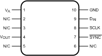
Pin Functions
| PIN | I/O | DESCRIPTION | |
|---|---|---|---|
| NO. | NAME | ||
| 1 | VA | — | Power supply and reference input; must be decoupled to GND |
| 2 | N/C | — | No connect; pin not internally connected to die |
| 3 | N/C | — | No connect; pin not internally connected to die |
| 4 | VOUT | Output | DAC analog output voltage |
| 5 | N/C | — | No connect; pin not internally connected to die |
| 6 | N/C | — | No connect; pin not internally connected to die |
| 7 | SYNC | Input | Frame synchronization input for the data input. When this pin goes low, it enables the input shift register and data is transferred on the falling edges of SCLK. The DAC is updated on the 16th clock cycle unless SYNC is brought high before the 16th clock, in which case the rising edge of SYNC acts as an interrupt and the write sequence is ignored by the DAC. |
| 8 | SCLK | Input | Serial clock input; data is clocked into the input shift register on the falling edges of this pin. |
| 9 | DIN | Input | Serial data input; data is clocked into the 16-bit shift register on the falling edges of SCLK after the fall of SYNC. |
| 10 | GND | — | Ground reference for all on-chip circuitry |
6 Specifications
6.1 Absolute Maximum Ratings(1)(2)
| MIN | MAX | UNIT | ||
|---|---|---|---|---|
| Supply voltage, VA | 6.5 | V | ||
| Voltage on any input pin | −0.3 | (VA + 0.3) | V | |
| Input current at any pin(3) | 10 | mA | ||
| Maximum output current(4) | 10 | mA | ||
| VOUT pin in power-down mode | 1 | mA | ||
| Package input current(3) | 20 | mA | ||
| Power dissipation at TA = 25°C | See(5) | |||
| Maximum junction temperature | 175 | °C | ||
| Lead temperature | CFP package (Soldering 10 Seconds) |
260 | °C | |
| Package weight (typical) | CFP package | 220 | mg | |
| Storage temperature, Tstg | −65 | 150 | °C | |
(360 Ω at VDD = 3.6 V).
6.2 ESD Ratings
| VALUE | UNIT | |||
|---|---|---|---|---|
| V(ESD) | Electrostatic discharge | Human-body model (HBM), per ANSI/ESDA/JEDEC JS-001(1)(2) | ±5000 | V |
6.3 Recommended Operating Conditions
| MIN | MAX | UNIT | |
|---|---|---|---|
| Operating temperature | −55 | 125 | °C |
| Supply voltage, VA | 2.7 | 5.5 | V |
| Any input voltage(1) | −0.1 | (VA + 0.1) | V |
| Output load | 0 | 1500 | pF |
| SCLK frequency | 20 | MHz |

6.4 Thermal Information
| THERMAL METRIC(1)(2) | DAC121S101QML-SP | UNIT | |
|---|---|---|---|
| NAC (CFP) | |||
| 10 PINS | |||
| RθJA | Junction-to-ambient thermal resistance | 214 | °C/W |
| RθJC(bot) | Junction-to-case (bottom) thermal resistance | 25.7 | °C/W |
6.5 DAC121S101QML-SP Electrical Characteristics DC Parameters
The following specifications apply for VA = 2.7 V to 5.5 V, RL = ∞, CL = 200 pF to GND, fSCLK = 20 MHz, input code range 48 to 4047. All limits TA = 25°C, unless otherwise specified.| PARAMETER | TEST CONDITIONS | NOTES | SUB-GROUPS | MIN | TYP(1) | MAX | UNIT | ||
|---|---|---|---|---|---|---|---|---|---|
| STATIC PERFORMANCE | |||||||||
| Resolution | TMIN ≤ TA ≤ TMAX | See(2) | 12 | Bits | |||||
| Monotonicity | TMIN ≤ TA ≤ TMAX | See(2) | 12 | Bits | |||||
| INL | Integral non-linearity | Over Decimal codes 48 to 4047 | [1, 2, 3] | −8 | ±2.75 | 8 | LSB | ||
| DNL | Differential non-linearity | VA = 2.7 V to 5.5 V | DNL MAX | [1, 2, 3] | 0.21 | 1 | LSB | ||
| DNL MIN | −0.7 | −0.1 | |||||||
| ZE | Zero code error | IOUT = 0 | [1, 2, 3] | 2.12 | 15 | mV | |||
| FSE | Full-scale error | IOUT = 0 | [1, 2, 3] | −0.04 | −1 | %FSR | |||
| GE | Gain error | All ones Loaded to DAC register | [1, 2, 3] | −0.11 | ±1 | %FSR | |||
| ZCED | Zero code error drift | See(2) | −20 | µV/°C | |||||
| TC GE | Gain error tempco | VA = 3 V | See(2) | −0.7 | ppm/°C | ||||
| VA = 5 V | −1 | ||||||||
| OUTPUT CHARACTERISTICS | |||||||||
| IPD SINK | Vout pin in power-down mode | All PD Modes, TMIN ≤ TA ≤ TMAX | See(2) | 1 | mA | ||||
| Output voltage range | TMIN ≤ TA ≤ TMAX | See(2) | 0 | VA | V | ||||
| ZCO | Zero code output | VA = 3 V, IOUT = 10 µA | [1, 2, 3] | 2 | 6 | mV | |||
| VA = 3 V, IOUT = 100 µA | [1, 2, 3] | 4 | 10 | ||||||
| VA = 5 V, IOUT = 10 µA | [1, 2, 3] | 2 | 8 | ||||||
| VA = 5 V, IOUT = 100 µA | [1, 2, 3] | 4 | 9 | ||||||
| FSO | Full-scale output | VA = 3 V, IOUT = 10 µA | [1, 2, 3] | 2.99 | 2.997 | V | |||
| VA = 3 V, IOUT = 100 µA | [1, 2, 3] | 2.985 | 2.991 | ||||||
| VA = 5 V, IOUT = 10 µA | [1, 2, 3] | 4.985 | 4.994 | ||||||
| VA = 5 V, IOUT = 100 µA | [1, 2, 3] | 4.985 | 4.992 | ||||||
| Maximum load capacitance | RL = ∞ | See(2) | 1500 | pF | |||||
| RL = 2 kΩ | 1500 | ||||||||
| DC output impedance | [1, 2, 3] | 8 | 16 | Ω | |||||
| LOGIC INPUT | |||||||||
| IIN | Input current | [1, 2, 3] | −200 | 6 | 200 | nA | |||
| VIL | Input low voltage | VA = 5 V, TMIN ≤ TA ≤ TMAX | [1, 2, 3] | 0.8 | V | ||||
| VA = 3 V, TMIN ≤ TA ≤ TMAX | [1, 2, 3] | 0.5 | |||||||
| VIH | Input high voltage | VA = 5 V, TMIN ≤ TA ≤ TMAX | [1, 2, 3] | 2.4 | V | ||||
| VA = 3 V, TMIN ≤ TA ≤ TMAX | [1, 2, 3] | 2.1 | |||||||
| CIN | Input capacitance | See(2) | 5 | pF | |||||
| POWER REQUIREMENTS | |||||||||
| IA | Supply current (output unloaded) | Normal Mode 5.5 V fSCLK = 20 MHz |
[1, 2, 3] | 216 | 270 | µA | |||
| Normal Mode 3.6 V fSCLK = 20 MHz |
[1, 2, 3] | 145 | 200 | ||||||
| Normal Mode 5.5 V fSCLK = 10 MHz |
[1, 2, 3] | 185 | 230 | ||||||
| Normal Mode 3.6 V fSCLK = 10 MHz |
[1, 2, 3] | 132 | 175 | ||||||
| Normal Mode 5.5 V fSCLK = 0 |
[1, 2, 3] | 150 | 190 | ||||||
| Normal Mode 3.6 V fSCLK = 0 |
[1, 2, 3] | 115 | 160 | ||||||
| All PD Modes, 5.5 V fSCLK = 20 MHz |
[1, 2, 3] | 22 | 60 | ||||||
| All PD Modes, 3.6 V fSCLK = 20 MHz |
[1, 2, 3] | 12 | 30 | ||||||
| All PD Modes, 5.5 V fSCLK = 10 MHz |
[1, 2, 3] | 12 | 40 | ||||||
| All PD Modes, 3.6 V fSCLK = 10 MHz |
[1, 2, 3] | 6 | 20 | ||||||
| All PD Modes, 5.5 V fSCLK = 0 |
[1, 2, 3] | 0.006 | 1 | ||||||
| All PD Modes, 3.6 V fSCLK = 0 |
[1, 2, 3] | 0.004 | 1 | ||||||
| PC | Power consumption (output unloaded) | Normal Mode, 5.5 V fSCLK = 20 MHz |
[1, 2, 3] | 1.19 | 1.49 | mW | |||
| Normal Mode 3.6 V fSCLK = 20 MHz |
[1, 2, 3] | 0.52 | 0.72 | ||||||
| Normal Mode, 5.5 V fSCLK = 10 MHz |
[1, 2, 3] | 1.02 | 1.27 | ||||||
| Normal Mode 3.6 V fSCLK = 10 MHz |
[1, 2, 3] | 0.47 | 0.63 | ||||||
| Normal Mode, 5.5 V fSCLK = 0 |
[1, 2, 3] | 0.82 | 1.05 | ||||||
| Normal Mode 3.6 V fSCLK = 0 |
[1, 2, 3] | 0.41 | 0.58 | ||||||
| All PD Modes, 5.5 V fSCLK = 20 MHz |
[1, 2, 3] | 0.12 | 0.33 | ||||||
| All PD Modes, 3.6 V fSCLK = 20 MHz |
[1, 2, 3] | 0.07 | 0.11 | ||||||
| All PD Modes, 5.5 V fSCLK = 10 MHz |
[1, 2, 3] | 0.04 | 0.22 | ||||||
| All PD Modes, 3.6 V fSCLK = 10 MHz |
[1, 2, 3] | 0.02 | 0.08 | ||||||
| All PD Modes, 5.5 V fSCLK = 0 |
[1, 2, 3] | 0.033 | 5.5 | ||||||
| All PD Modes, 3.6 V fSCLK = 0 |
[1, 2, 3] | 0.014 | 3.6 | ||||||
| IOUT | Power efficiency | ILOAD = 2 mA | See(2) | 91% | |||||
| IA | 94% | ||||||||
6.6 DAC121S101QML-SP Electrical Characteristics AC and Timing Characteristics
The following specifications apply for VA = 2.7 V to 5.5 V, RL = ∞, CL = 200 pF to GND, fSCLK = 20 MHz, input code range 48 to 4047. All limits TA = 25°C, unless otherwise specified.| PARAMETER | TEST CONDITIONS | NOTES | SUB-GROUPS | MIN | TYP(1) | MAX | UNIT | |||
|---|---|---|---|---|---|---|---|---|---|---|
| fSCLK | SCLK frequency | (See Figure 31) | [9,10,11] | 20 | MHz | |||||
| ts | Output voltage settling time |
FF0 to 00F code change, RL = ∞ | CL ≤ 200 pF | [9,10,11] | 12.5 | 15 | µs | |||
| CL = 500 pF | [9,10,11] | 12.5 | 15 | |||||||
| 00Fh to FF0h code change, RL = ∞ | CL ≤ 200 pF | [9,10,11] | 12.5 | 15 | ||||||
| CL = 500 pF | [9,10,11] | 12.5 | 15 | |||||||
| SR | Output slew rate | See(2) | 1 | V/µs | ||||||
| Glitch impulse | Code change from 800h to 7FFh | See(2) | 12 | nV-sec | ||||||
| Digital feedthrough | See(2) | 0.5 | nV-sec | |||||||
| tWU | Wake-Up Time | VA = 5 V | See(2) | 0.65 | µs | |||||
| VA = 3 V | 1.1 | |||||||||
| 1/fSCLK | SCLK cycle time | (See Figure 31) | [9,10,11] | 50 | ns | |||||
| tH | SCLK high time | (See Figure 31) | [9,10,11] | 20 | ns | |||||
| tL | SCLK low time | (See Figure 31) | [9,10,11] | 20 | ns | |||||
| tSUCL | Setup time SYNC to SCLK rising edge | (See Figure 31) | [9,10,11] | 0 | ns | |||||
| tSUD | Data setup time | (See Figure 31) | [9,10,11] | 6 | ns | |||||
| tDHD | Data hold time | (See Figure 31) | [9,10,11] | 4.5 | ns | |||||
| tCS | SCLK fall to rise of SYNC | VA = 5.5 V (See Figure 31) | [9,10,11] | 10 | ns | |||||
| VA = 2.7 V (See Figure 31) | [9,10,11] | 18 | ||||||||
| tSYNC | SYNC high time | VA = 5.5 V (See Figure 31) | [9,10,11] | 37 | ns | |||||
| VA = 2.7 V (See Figure 31) | [9,10,11] | 36 | ||||||||
6.7 DAC121S101QML Electrical Characteristics Radiation Electrical Characteristics(1)
The following specifications apply for VA = 2.7 V to 5.5 V, RL = ∞, CL = 200 pF to GND, fSCLK = 20 MHz, input code range 48 to 4047.| PARAMETER | TEST CONDITIONS | SUB-GROUPS | MIN | MAX | UNIT | ||
|---|---|---|---|---|---|---|---|
| POWER REQUIREMENTS | |||||||
| IA | Supply current (output unloaded) | Normal Mode fSCLK = 20 MHz |
5.5 V | [1] | 325 | µA | |
| 3.6 V | [1] | 250 | |||||
| Normal Mode fSCLK = 10 MHz |
5.5 V | [1] | 300 | ||||
| 3.6 V | [1] | 225 | |||||
| Normal Mode fSCLK = 0 |
5.5 V | [1] | 275 | ||||
| 3.6 V | [1] | 200 | |||||
| All PD Modes, fSCLK = 20 MHz |
5.5 V | [1] | 125 | ||||
| 3.6 V | [1] | 100 | |||||
| All PD Modes, fSCLK = 10 MHz |
5.5 V | [1] | 115 | ||||
| 3.6 V | [1] | 95 | |||||
| All PD Modes, fSCLK = 0 |
5.5 V | [1] | 100 | ||||
| 3.6 V | [1] | 100 | |||||
6.8 DAC121S101QML-SP Electrical Characteristics Operating Life Test Delta Parameters
TA at 25°C(1)
| PARAMETER | TEST CONDITIONS | SUB-GROUPS | MIN | MAX | UNIT | |
|---|---|---|---|---|---|---|
| INL | Integral non-linearity | [1] | ±2 | LBS | ||
| ts | Output voltage settling time | [1] | ±5 | µA | ||
| IA | Supply current (output unloaded) | Normal Mode, VA = 5.5 V, fSCLK = 20 MHz | [1] | ±10 | µA | |
| Normal Mode, VA = 3.6 V, fSCLK = 20 MHz | [1] | ±6 | ||||
| Normal Mode, VA = 5.5 V, fSCLK = 10 MHz | [1] | ±10 | ||||
| Normal Mode, VA = 3.6 V, fSCLK = 10 MHz | [1] | ±6 | ||||
| Normal Mode, VA = 5.5 V, fSCLK = 0 | [1] | ±8 | ||||
| Normal Mode, VA = 3.6 V, fSCLK = 0 | [1] | ±6 | ||||
| All PD Modes, VA = 5.5 V, fSCLK = 20 MHz | [1] | ±2 | ||||
| All PD Modes, VA = 3.6 V, fSCLK = 20 MHz | [1] | ±1 | ||||
| All PD Modes, VA = 5.5 V, fSCLK = 10 MHz | [1] | ±1 | ||||
| All PD Modes, VA = 3.6 V, fSCLK = 10 MHz | [1] | ±1 | ||||
| All PD Modes, VA = 5.5 V, fSCLK = 0 | [1] | ±0.1 | ||||
| All PD Modes, VA = 3.6 V, fSCLK = 0 | [1] | ±0.1 | ||||
The DAC121S101QML-SP operates over the extended temperature range of –55°C to +125°C.
See Radiation Environments for dose rate environment information.
Table 1. Quality Conformance Inspection(1)
| SUB-GROUP | DESCRIPTION | TEMP (°C) |
|---|---|---|
| 1 | Static tests at | +25 |
| 2 | Static tests at | +125 |
| 3 | Static tests at | –55 |
| 4 | Dynamic tests at | +25 |
| 5 | Dynamic tests at | +125 |
| 6 | Dynamic tests at | –55 |
| 7 | Functional tests at | +25 |
| 8A | Functional tests at | +125 |
| 8B | Functional tests at | –55 |
| 9 | Switching tests at | +25 |
| 10 | Switching tests at | +125 |
| 11 | Switching tests at | –55 |
| 12 | Setting time at | +25 |
| 13 | Setting time at | +125 |
| 14 | Setting time at | –55 |
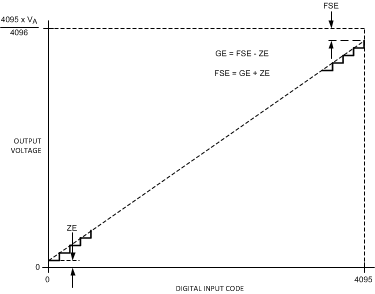 Figure 1. Input / Output Transfer Characteristic
6.9 Typical Characteristics
fSCLK = 20 MHz, TA = 25°C, Input Code Range 48 to 4047, unless otherwise stated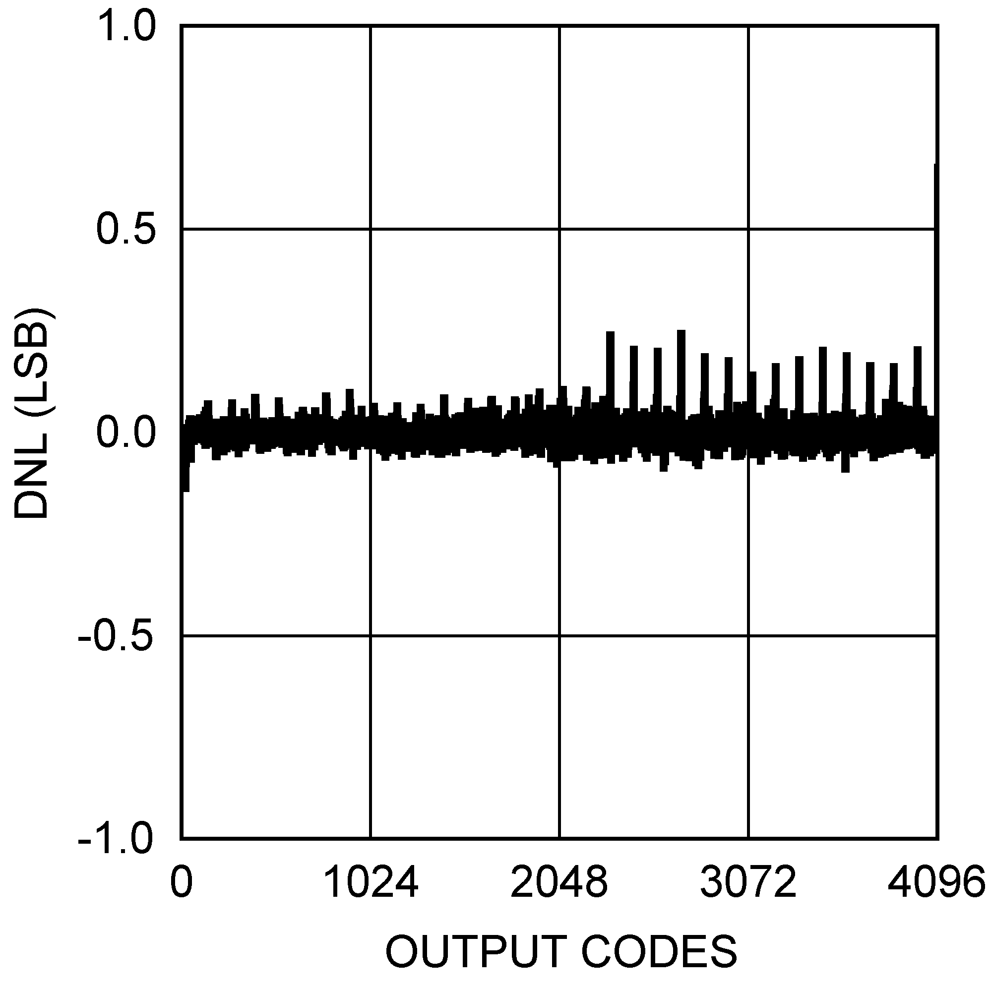 Figure 2. DNL at VA = 2.7 V
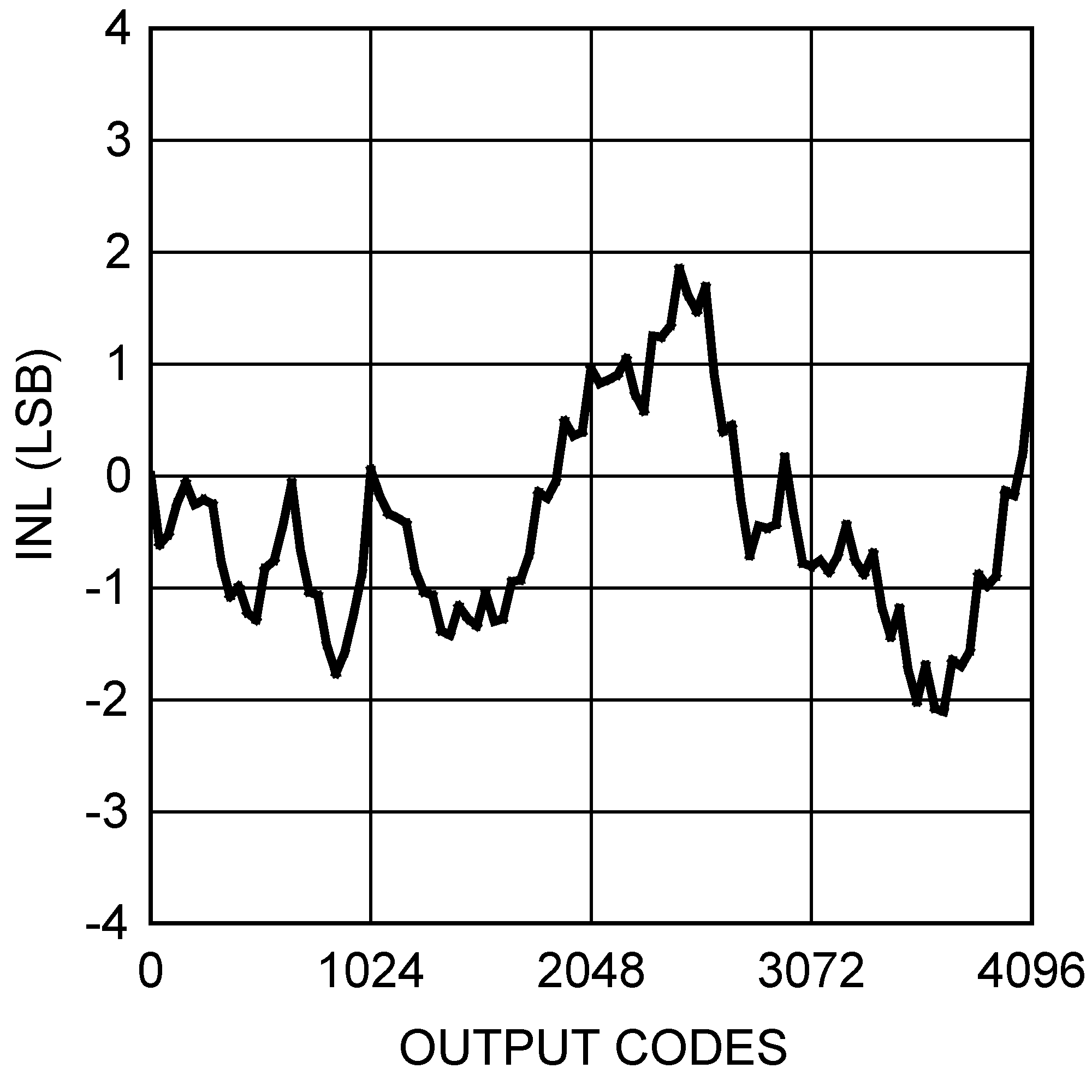 Figure 4. INL at VA = 2.7 V
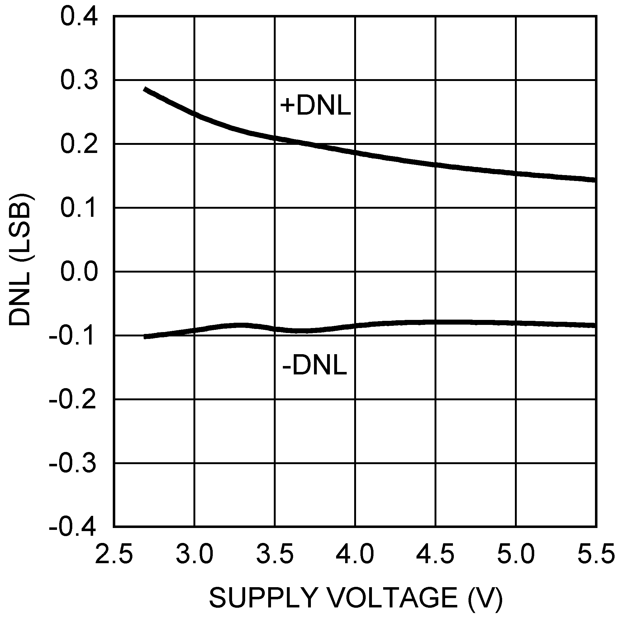 Figure 6. DNL vs VA
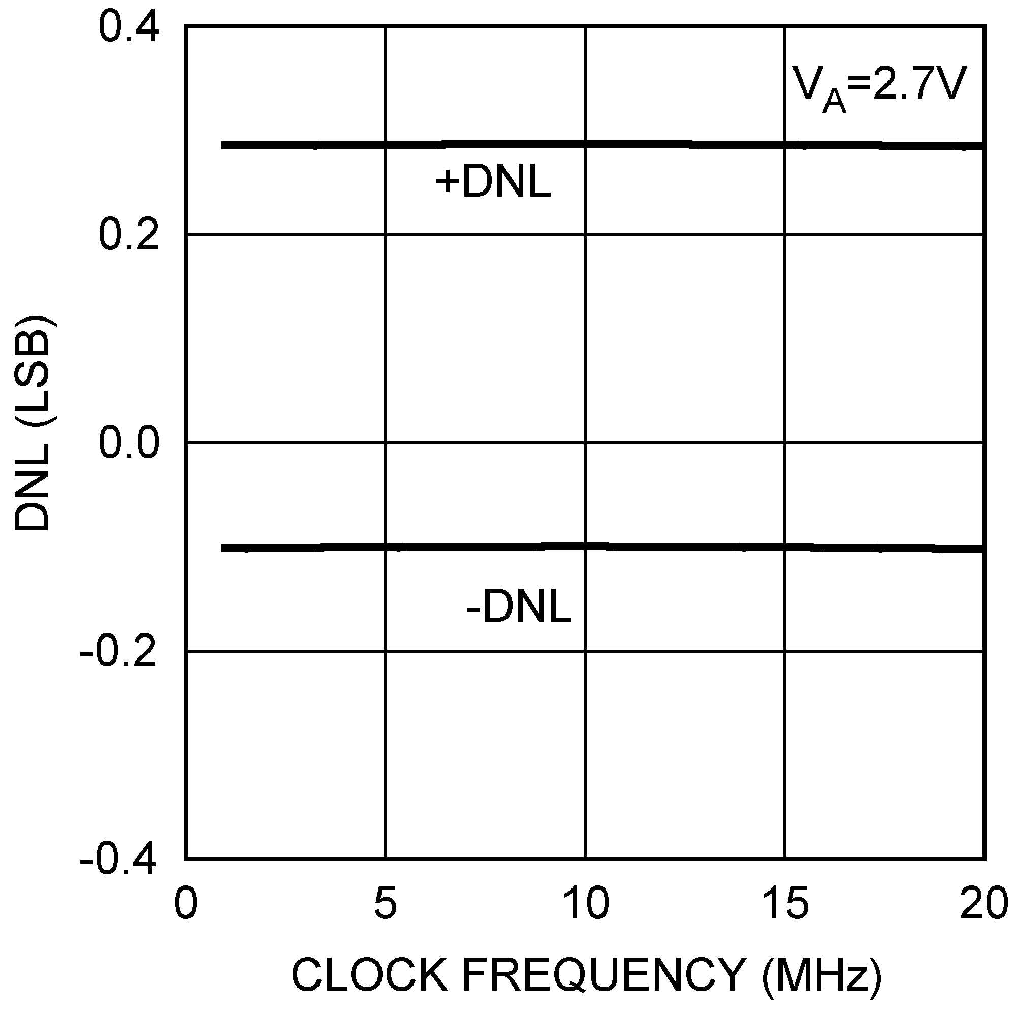 Figure 8. 2.7-V DNL vs fSCLK
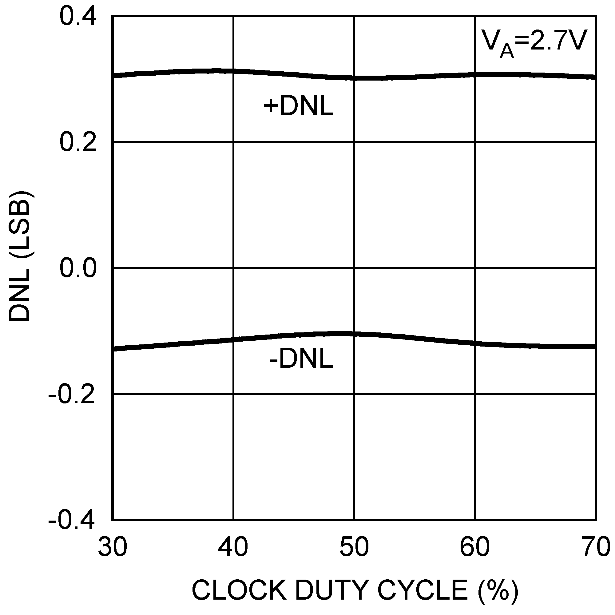 Figure 10. 2.7-V DNL vs Clock Duty Cycle
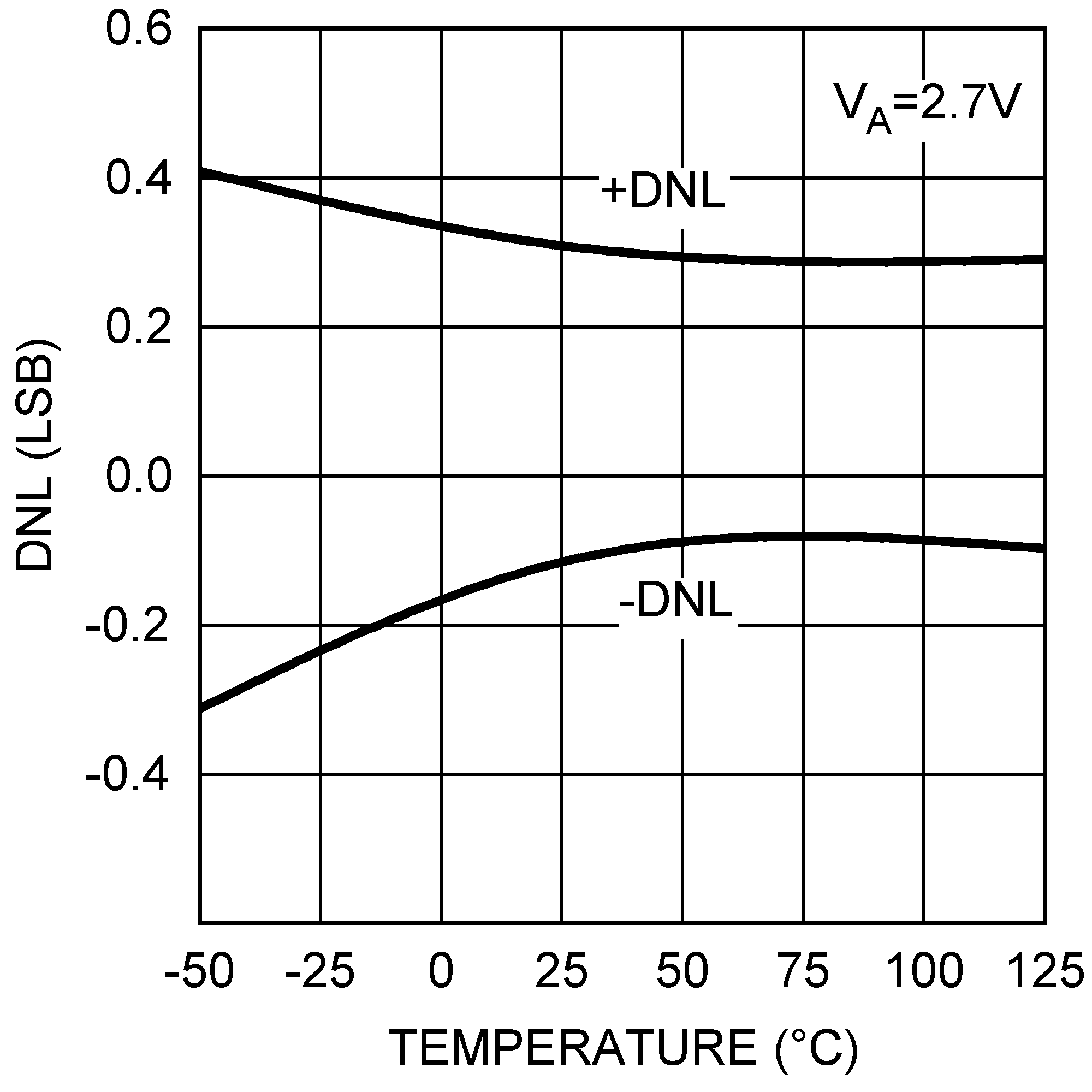 Figure 12. 2.7-V DNL vs Temperature
 Figure 14. 2.7-V INL vs fSCLK
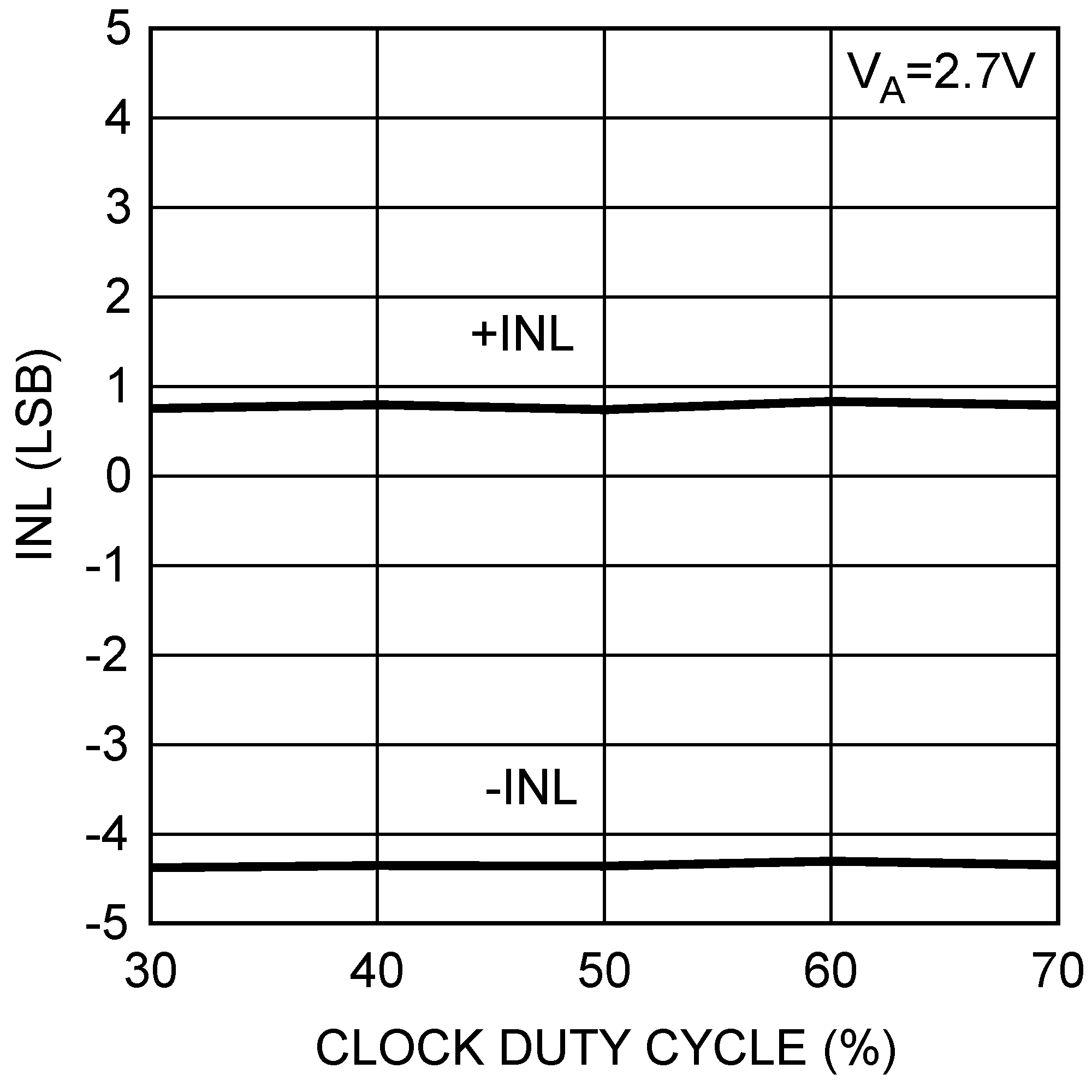 Figure 16. 2.7-V INL vs Clock Duty Cycle
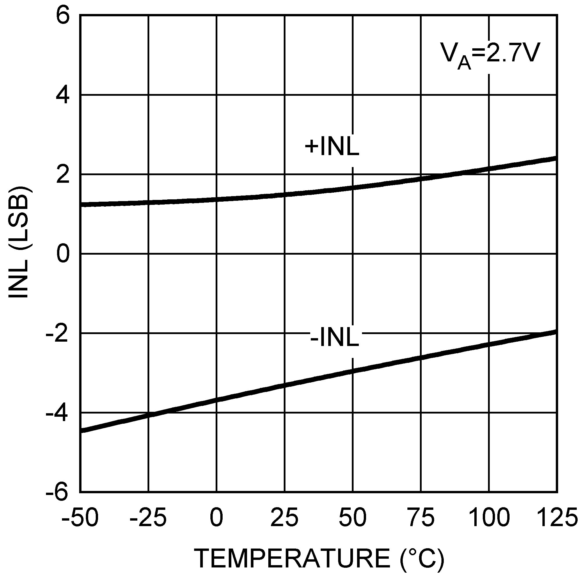 Figure 18. 2.7-V INL vs Temperature
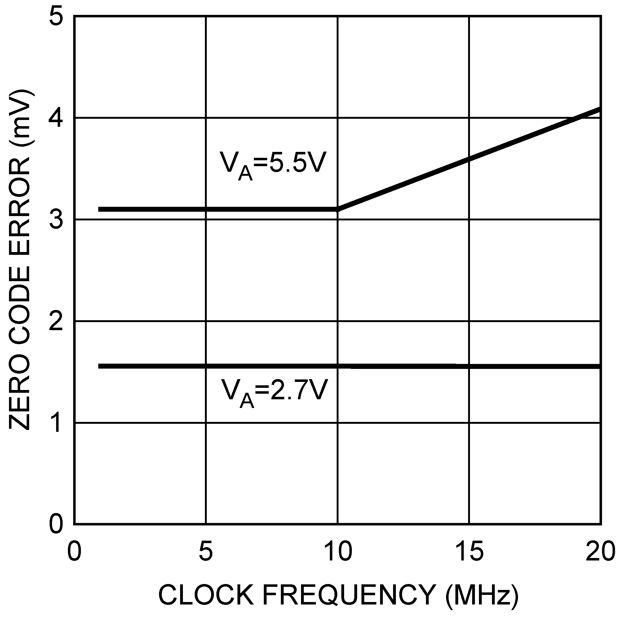 Figure 20. Zero Code Error vs fSCLK
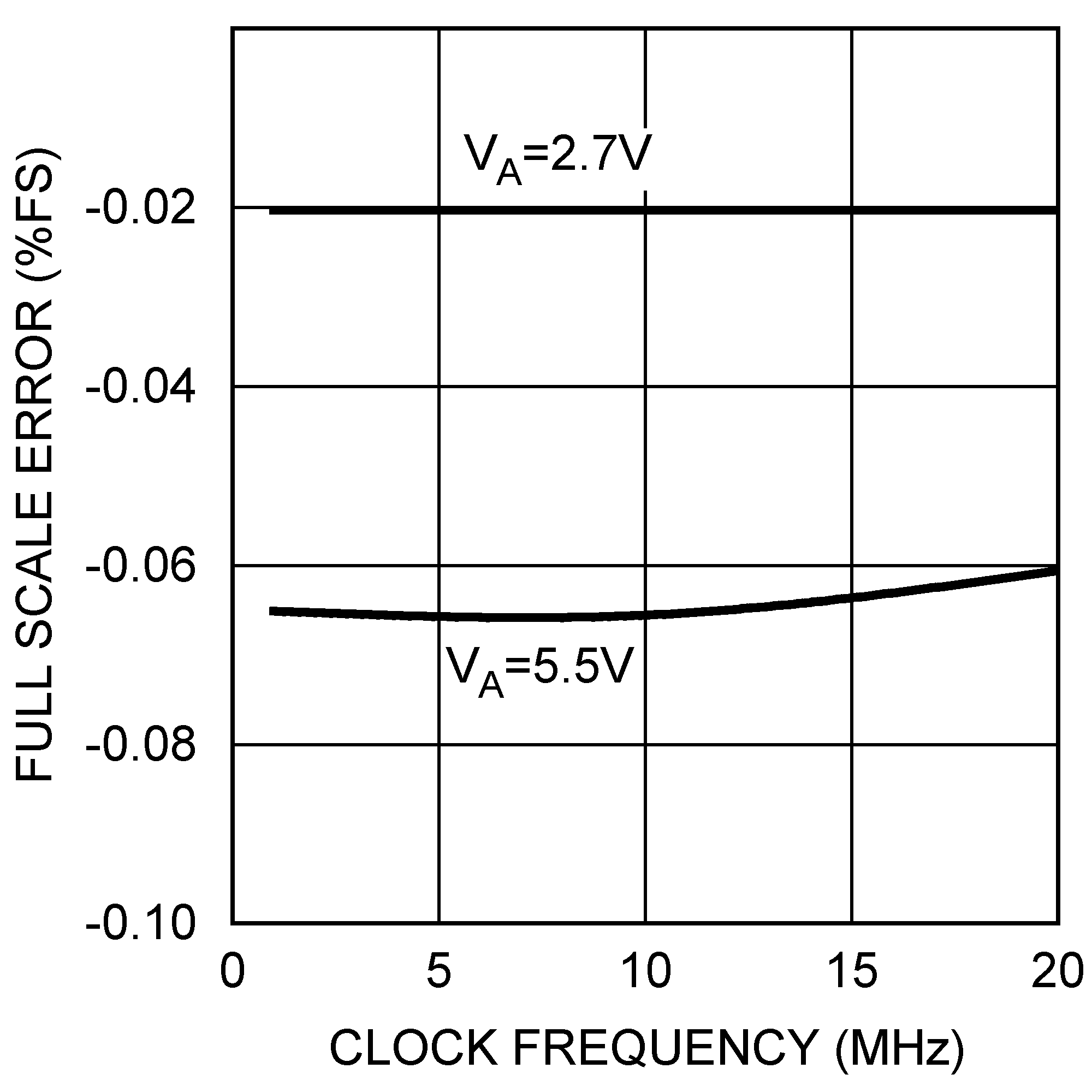 Figure 22. Full-Scale Error vs fSCLK
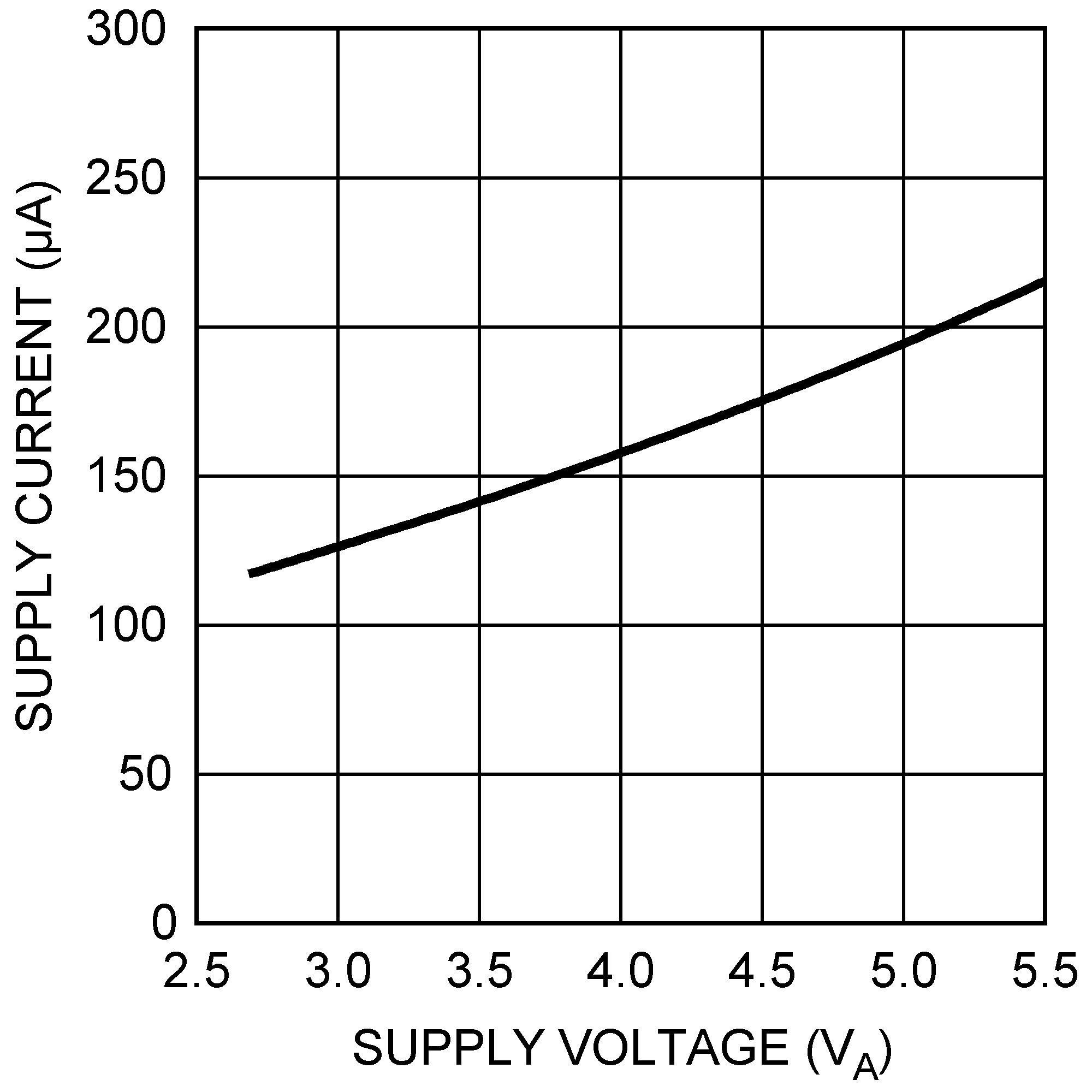 Figure 24. Supply Current vs VA
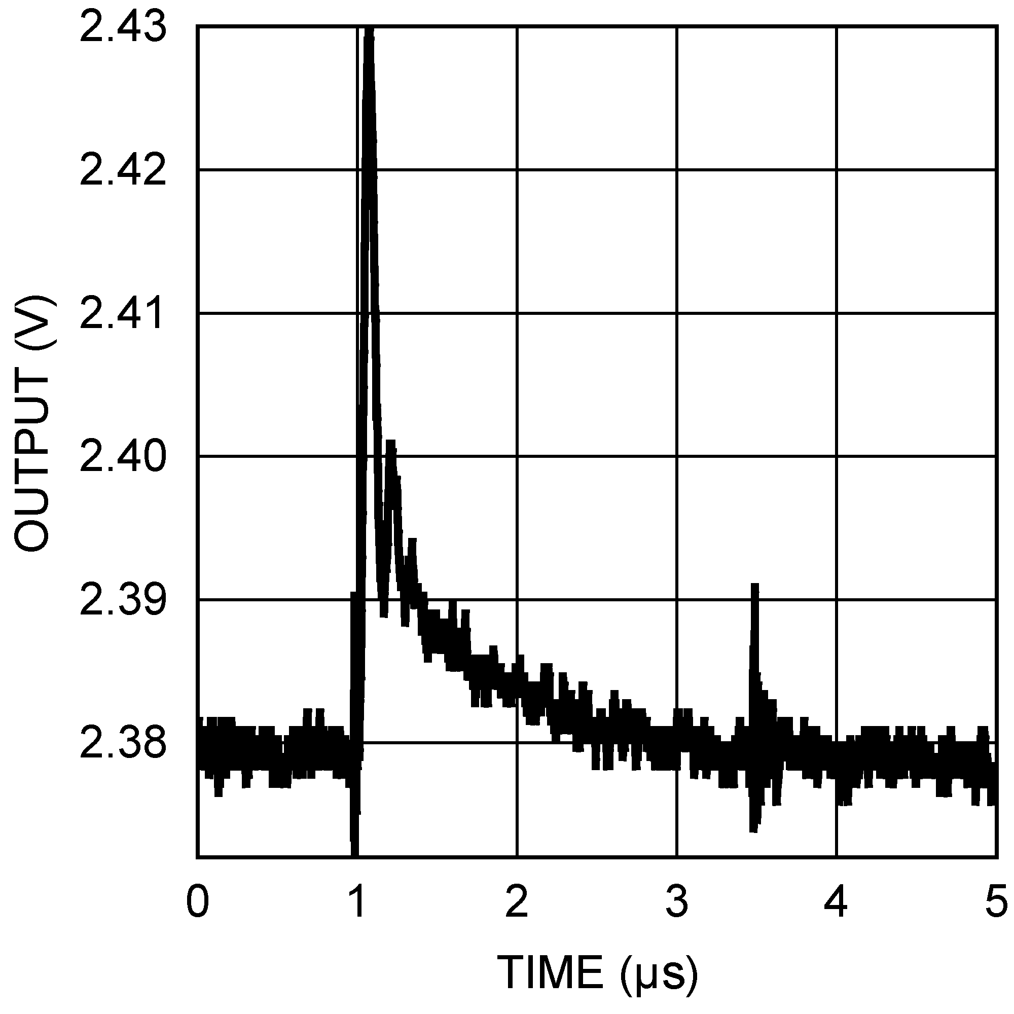 Figure 26. 5-V Glitch Response
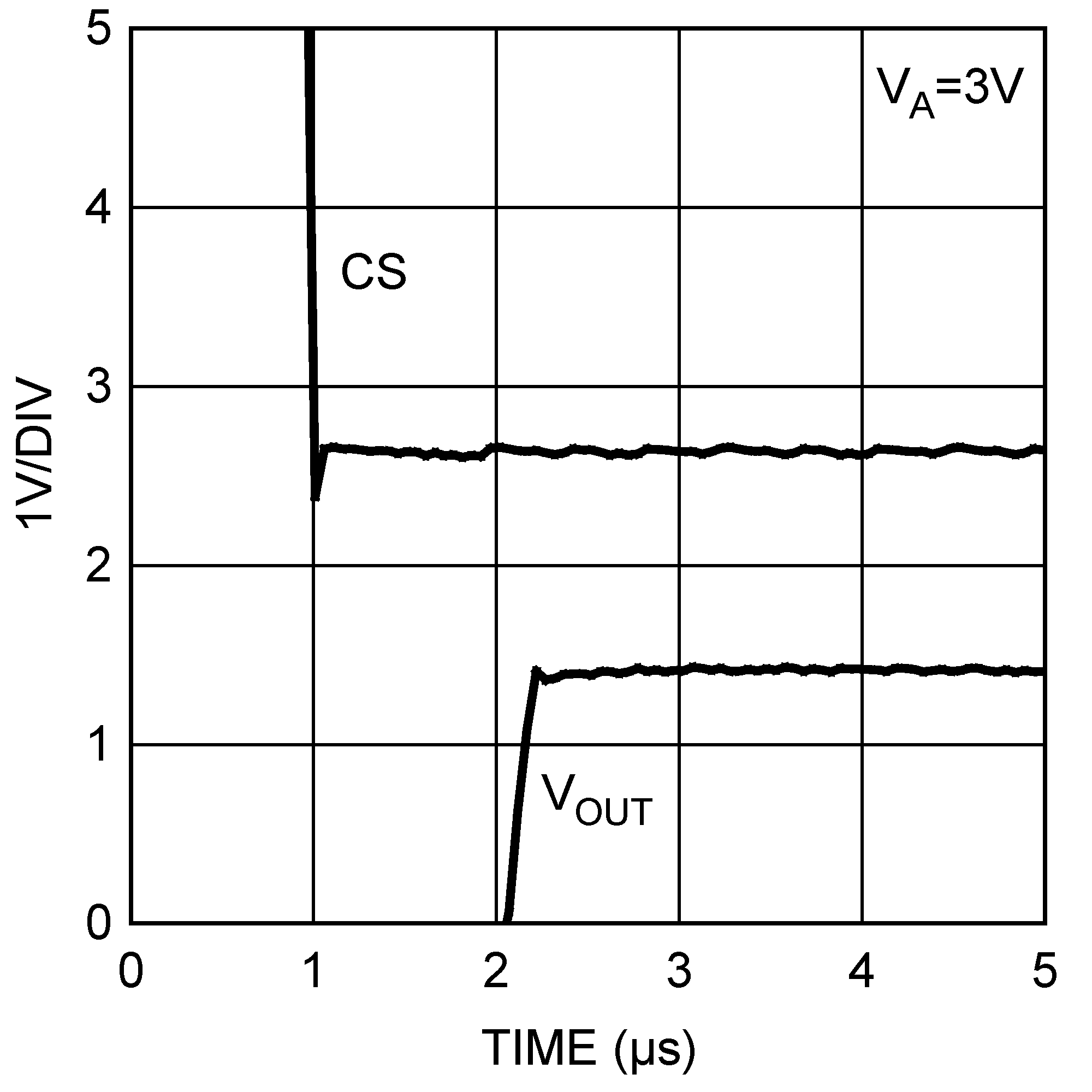 Figure 28. 3-V Wake-Up Time
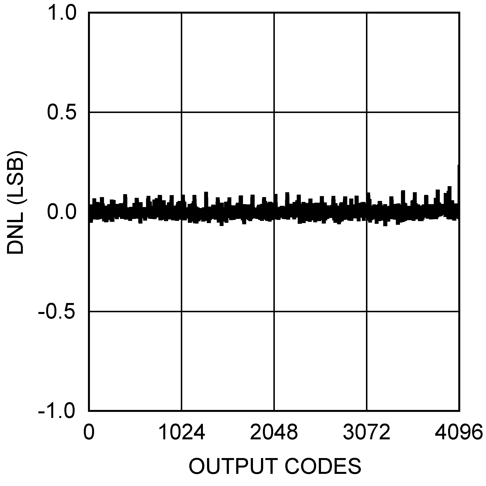 Figure 3. DNL at VA = 5.5 V
 Figure 5. INL at VA = 5.5 V
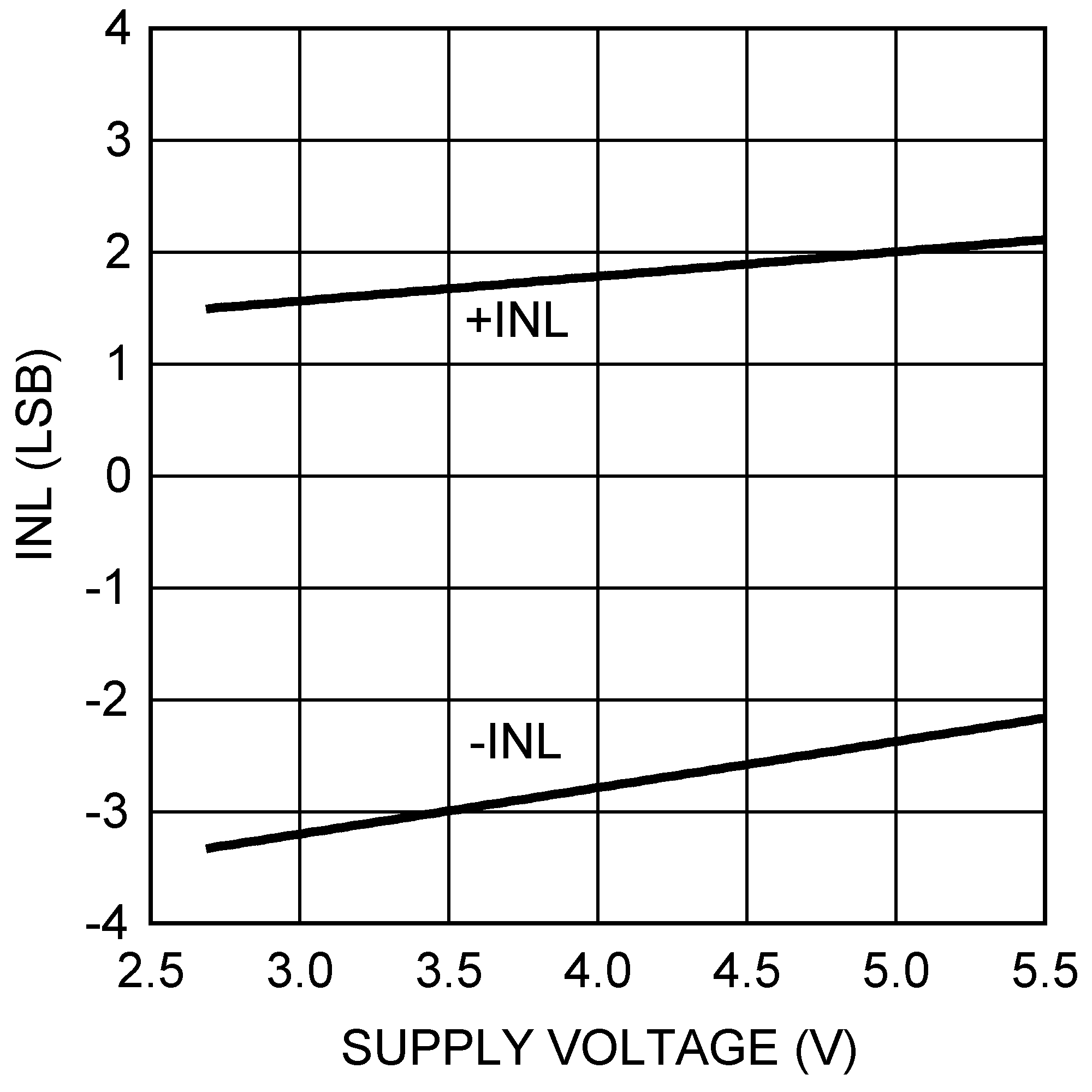 Figure 7. INL vs VA
 Figure 9. 5.5-V DNL vs fSCLK
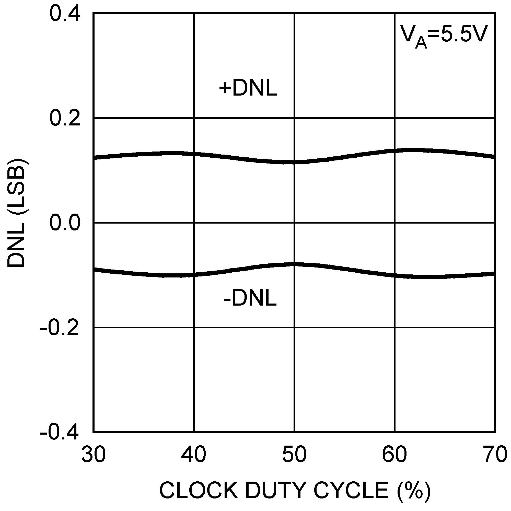 Figure 11. 5.5-V DNL vs Clock Duty Cycle
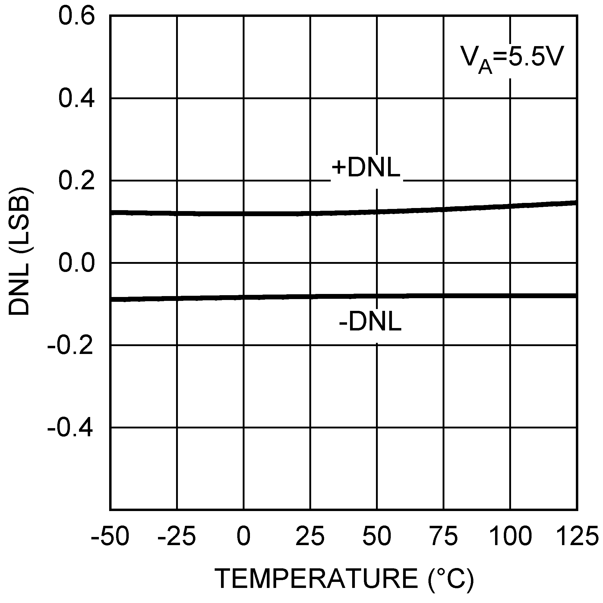 Figure 13. 5.5-V DNL vs Temperature
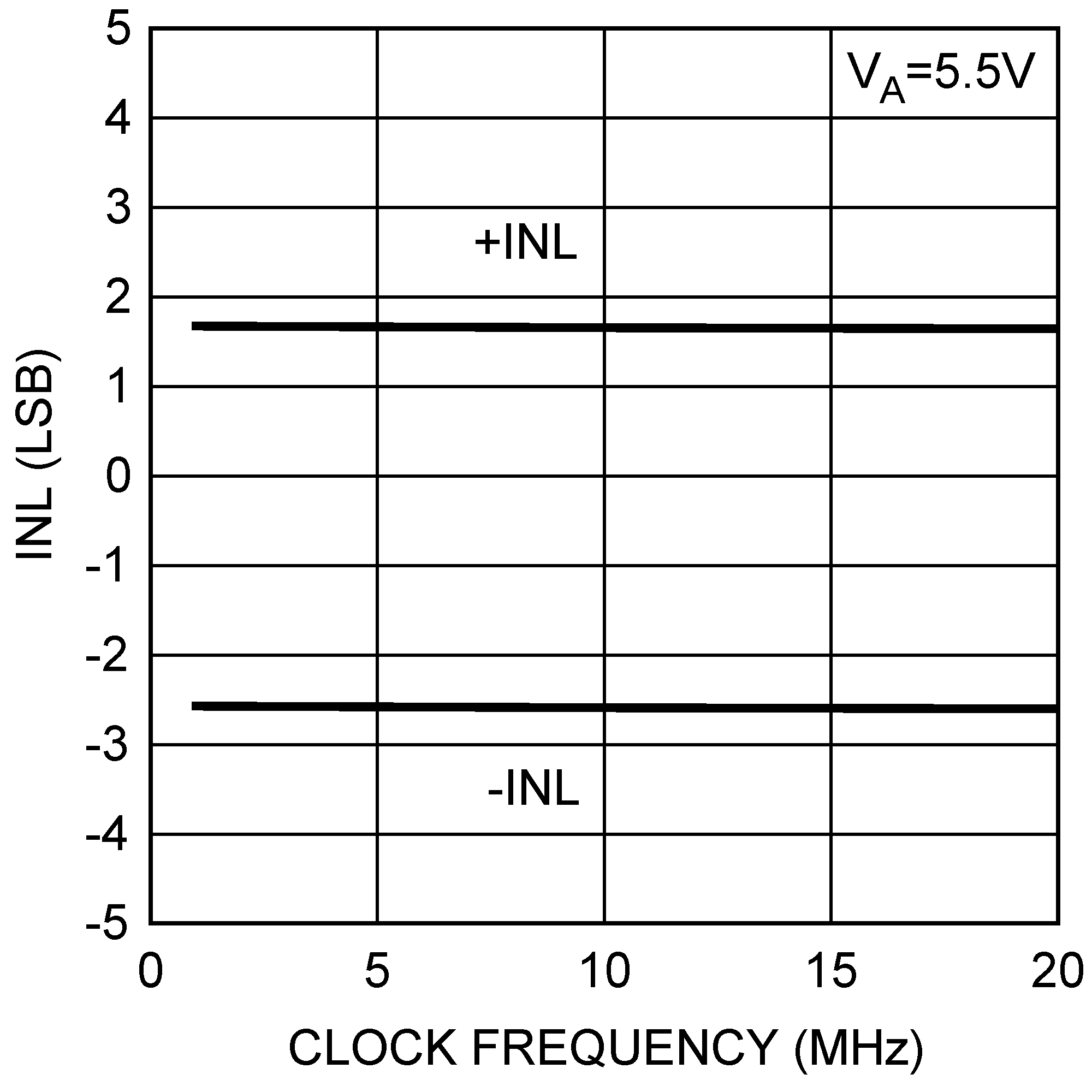 Figure 15. 5.5-V INL vs fSCLK
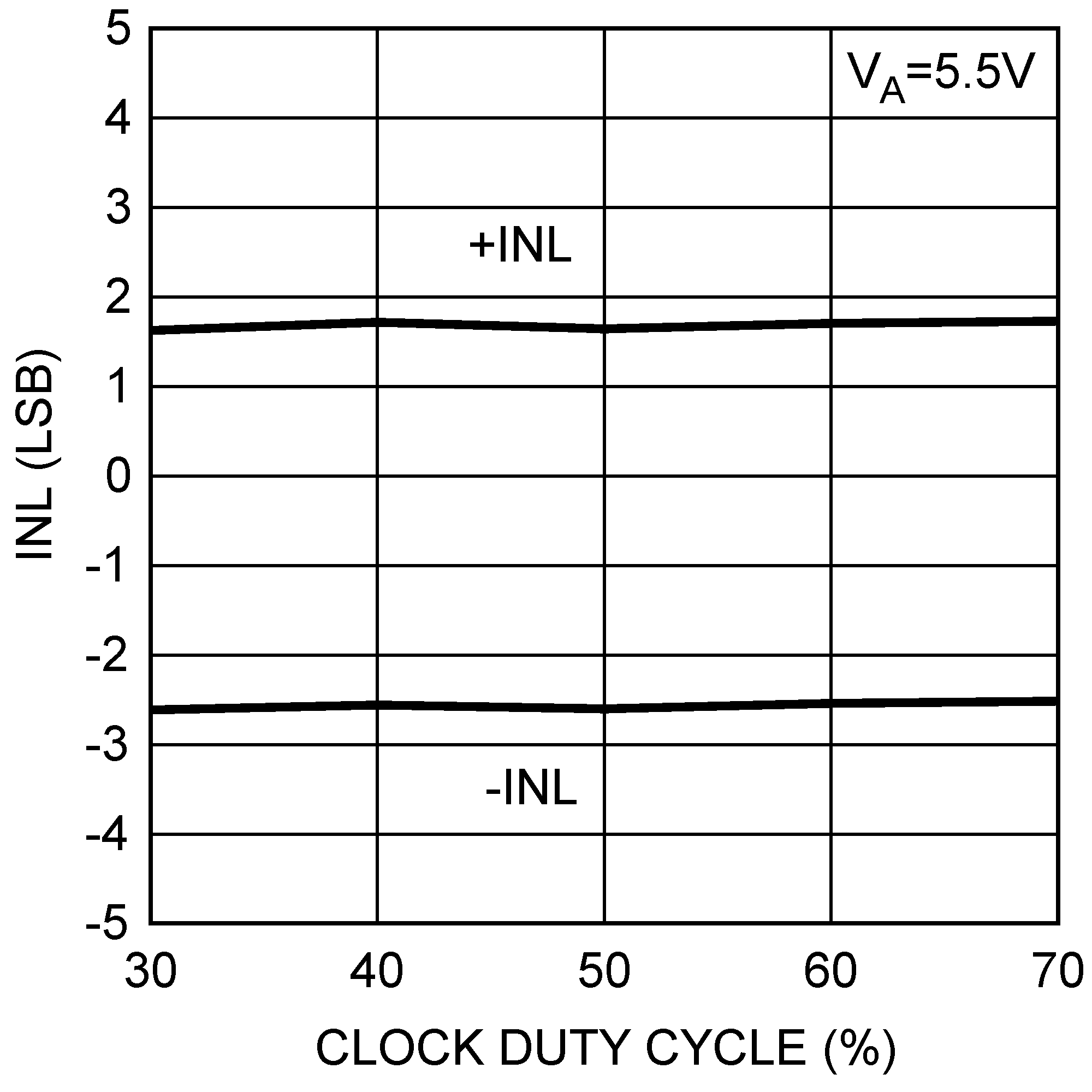 Figure 17. 5.5-V INL vs Clock Duty Cycle
 Figure 19. 5.5-V INL vs Temperature
 Figure 21. Zero Code Error vs Temperature
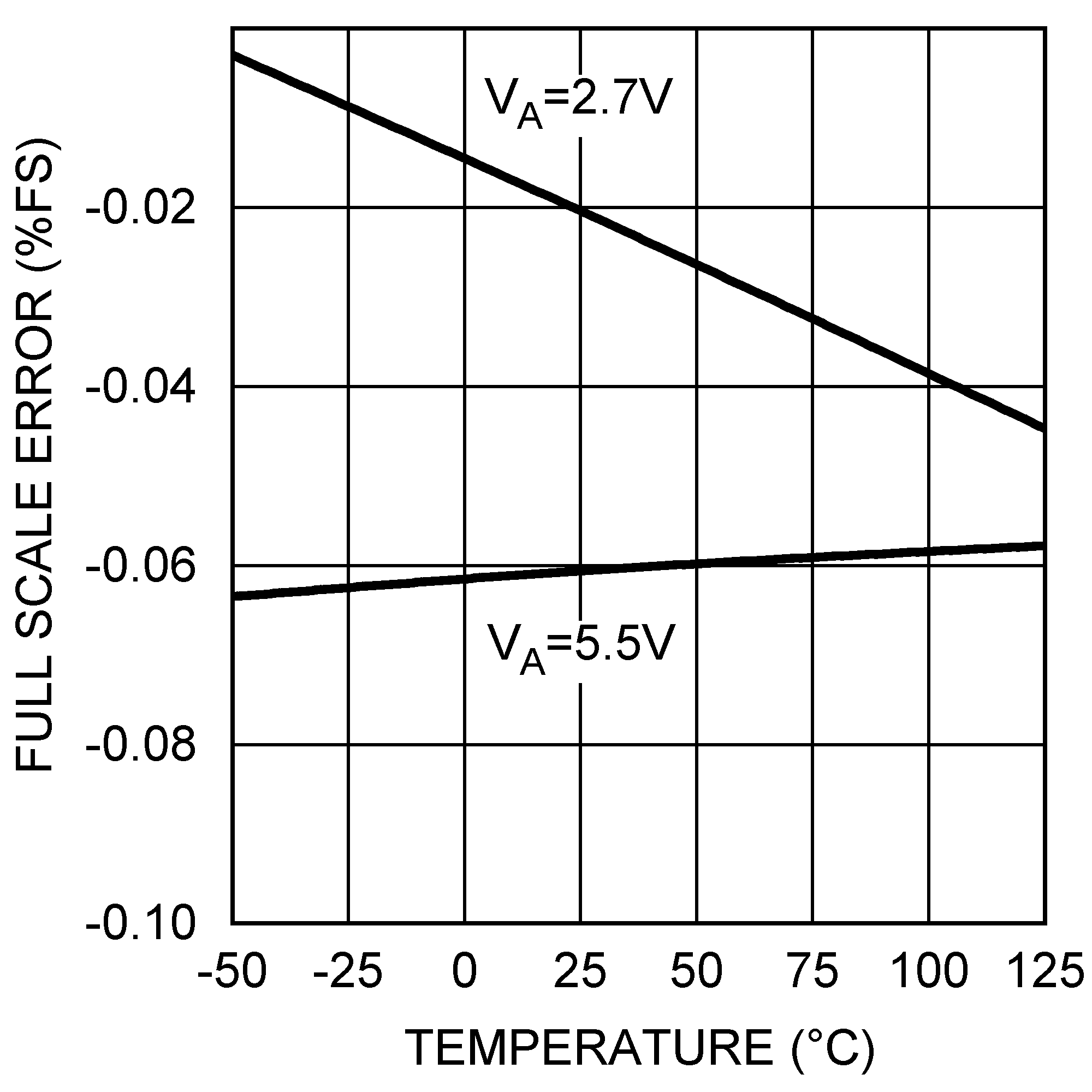 Figure 23. Full-Scale Error vs Temperature
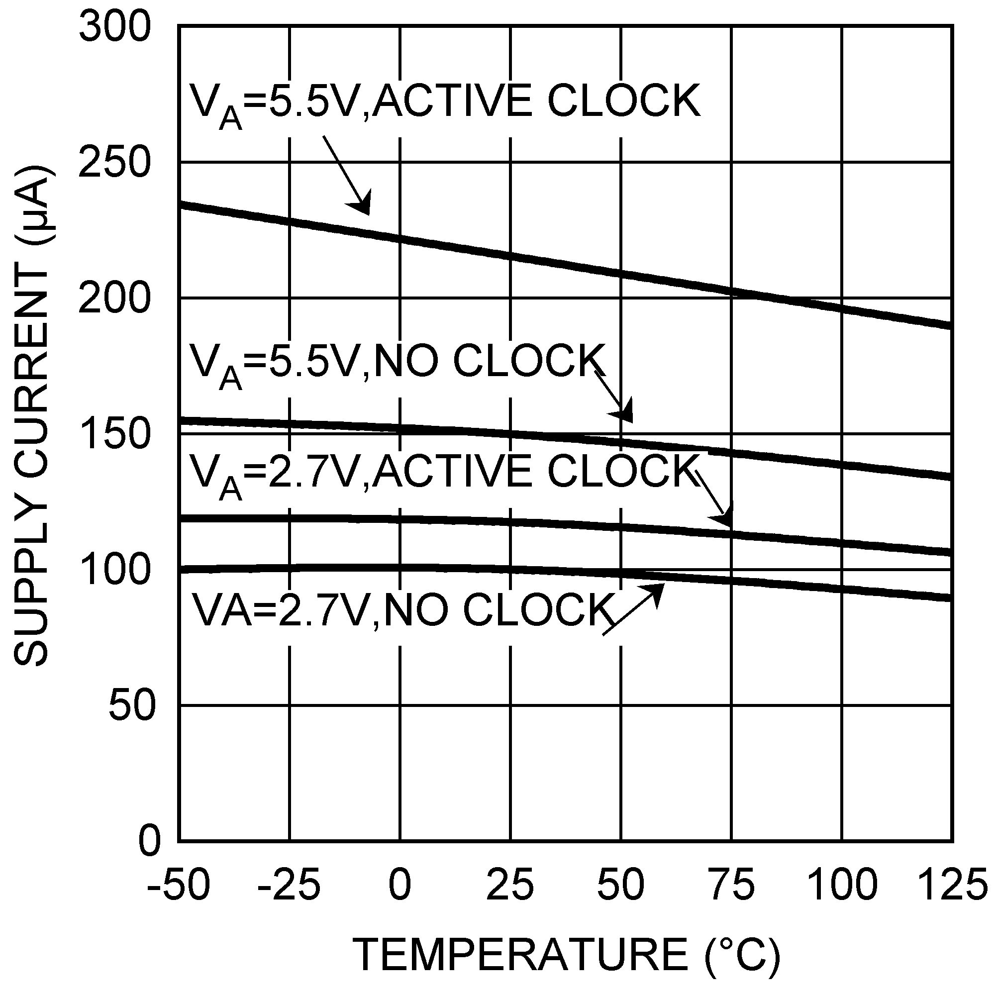 Figure 25. Supply Current vs Temperature
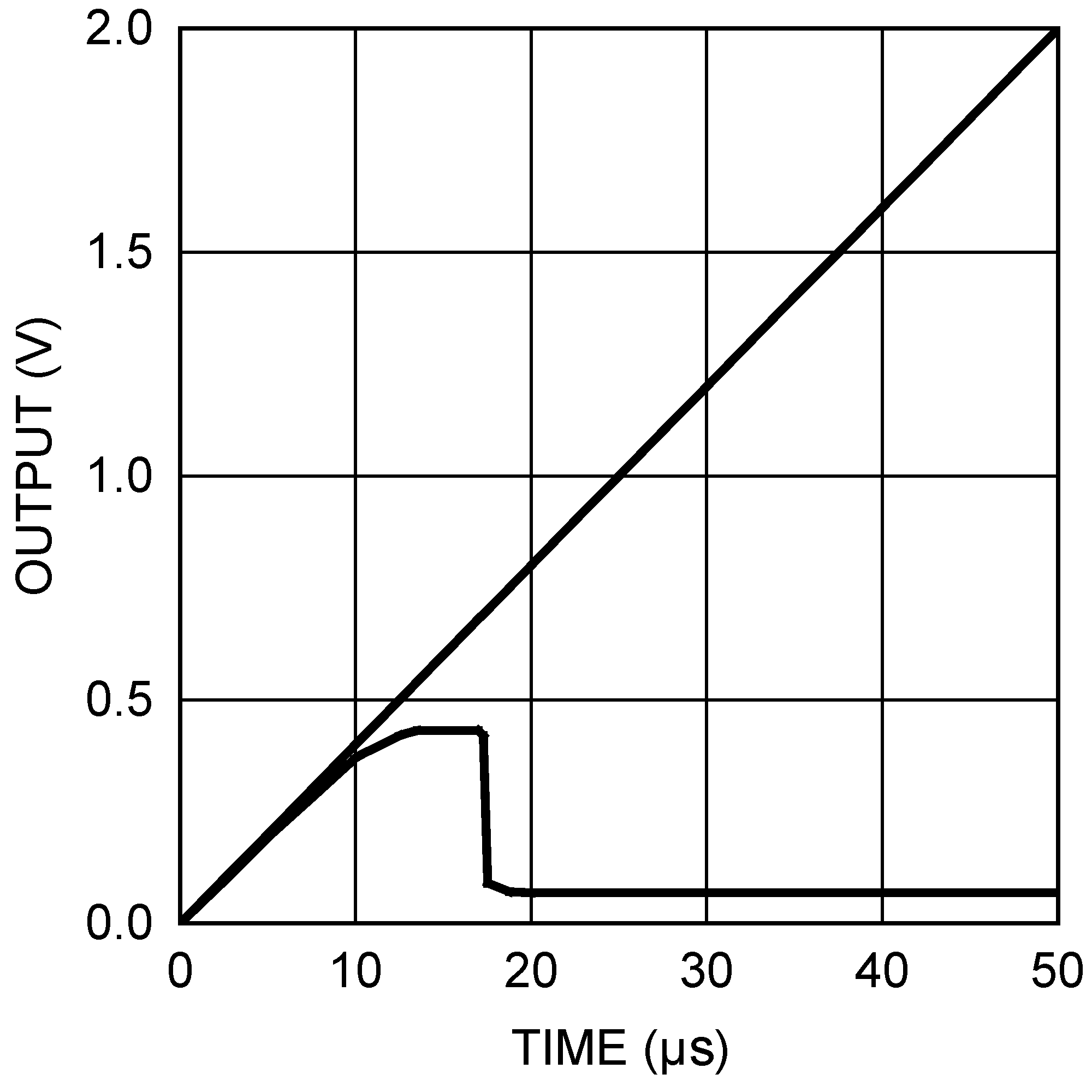 Figure 27. Power-On Reset
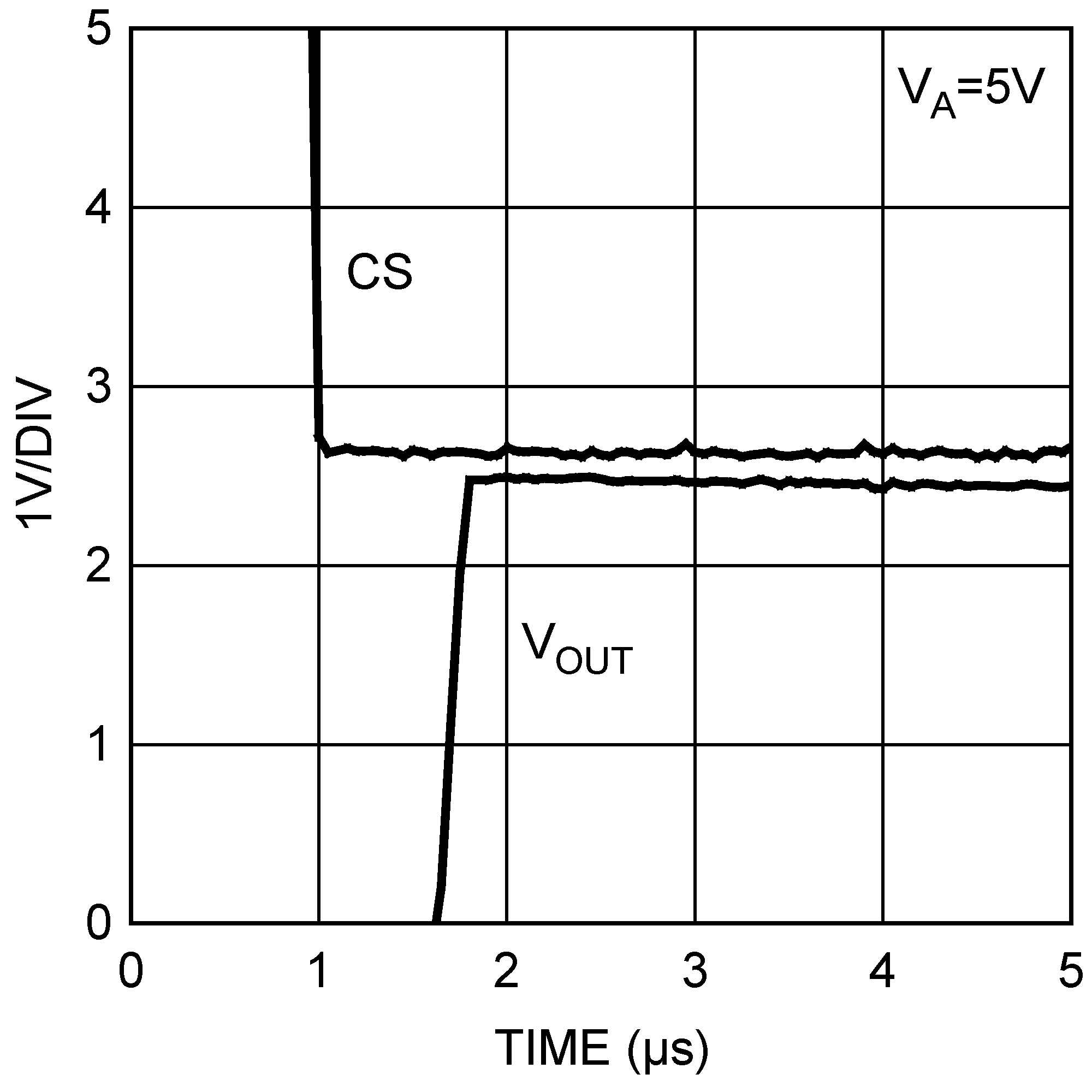 Figure 29. 5-V Wake-Up Time
7 Detailed Description
7.1 Overview
The DAC121S101QML-SP device is a full-featured, general purpose 12-bit voltage-output digital-to-analog converter (DAC). Control of the output of the DAC is achieved over a 3-wire SPI interface. Once the DAC output has been set, additional communication with the DAC is not required unless the output condition needs to be changed. Likewise, the DAC121S101QML-SP power-on state is 0 V. The DAC output will remain at 0 V until a valid write sequence is made.
7.2 Functional Block Diagram

7.3 Feature Description
7.3.1 DAC Section
The DAC121S101QML-SP is fabricated on a CMOS process with an architecture that consists of switches and a resistor string that are followed by an output buffer. The power supply serves as the reference voltage. The input coding is straight binary with an ideal output voltage of:
where
- D is the decimal equivalent of the binary code that is loaded into the DAC register and can take on any value between 0 and 4095.
7.3.2 Resistor String
Figure 30 shows the simplified resistor string. Conceptually, this string consists of 4096 equal valued resistors with a switch at each junction of two resistors, plus a switch to ground. The code loaded into the DAC register determines which switch is closed, connecting the proper node to the amplifier. This configuration ensures that the DAC is monotonic.
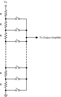 Figure 30. DAC Resistor String
7.3.3 Output Amplifier
The output buffer amplifier is a rail-to-rail type, providing an output voltage range of 0 V to VA. All amplifiers, even rail-to-rail types, exhibit a loss of linearity as the output approaches the supply rails (0 V and VA, in this case). For this reason, linearity is specified over less than the full output range of the DAC. The output capabilities of the amplifier are described in the electrical tables in Specifications.
7.3.4 Power-On Reset
The power-on reset circuit controls the output voltage during power-up. Upon application of power, the DAC register is filled with zeros and the output voltage is 0 V and remains there until a valid write sequence is made to the DAC.
7.4 Device Functional Modes
7.4.1 Power-Down Modes
The DAC121S101QML-SP has four modes of operation. These modes are set with two bits (DB13 and DB12) in the control register.
Table 2. Modes of Operation
| DB13 | DB12 | OPERATING MODE |
| 0 | 0 | Normal Operation |
| 0 | 1 | Power Down with 5 kΩ to GND |
| 1 | 0 | Power Down with 100 kΩ to GND |
| 1 | 1 | Power Down with Hi-Z |
When both DB13 and DB12 are 0, the device operates normally. For the other three possible combinations of these bits the supply current drops to its power-down level and the output is pulled down with either a 5-kΩ or a 100-kΩ resistor, or is in a high impedance state, as described in Table 2.
The bias generator, output amplifier, the resistor string, and other linear circuitry are all shut down in any of the power-down modes. Minimum power consumption is achieved in the power-down mode with SCLK disabled and SYNC and DIN idled low.
7.5 Programming
7.5.1 Serial Interface
The three-wire interface is compatible with SPI, QSPI, and MICROWIRE, as well as most DSPs. See Figure 31 for information on a write sequence.
A write sequence begins by bringing the SYNC line low. When SYNC is low, the data on the DIN line is clocked into the 16-bit serial input register on the falling edges of SCLK. On the 16th falling clock edge, the last data bit is clocked in and the programmed function (a change in the mode of operation or a change in the DAC register contents) is executed. At this point the SYNC line may be kept low or brought high. In either case, it must be brought high for the minimum specified time before the next write sequence as a falling edge of SYNC can initiate the next write cycle.
Because the SYNC and DIN buffers draw more current when they are high, they must be idled low between write sequences to minimize power consumption.
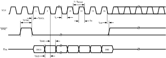 Figure 31. DAC121S101QML-SP Timing
7.5.2 Input Shift Register
The input shift register, Figure 32, has 16 bits. The first two bits are don't cares and are followed by two bits that determine the mode of operation (normal mode or one of three power-down modes). The contents of the serial input register are transferred to the DAC register on the sixteenth falling edge of SCLK. See the timing diagram, Figure 31.
 Figure 32. Input Register Contents
Normally, the SYNC line is kept low for at least 16 falling edges of SCLK and the DAC is updated on the 16th SCLK falling edge. However, if SYNC is brought high before the 16th falling edge, the shift register is reset and the write sequence is invalid. The DAC register is not updated and there is no change in the mode of operation or in the output voltage.