SNAS410F May 2008 – July 2016 DAC121S101QML-SP
PRODUCTION DATA.
- 1 Features
- 2 Applications
- 3 Description
- 4 Revision History
- 5 Pin Configuration and Functions
-
6 Specifications
- 6.1 Absolute Maximum Ratings
- 6.2 ESD Ratings
- 6.3 Recommended Operating Conditions
- 6.4 Thermal Information
- 6.5 DAC121S101QML-SP Electrical Characteristics DC Parameters
- 6.6 DAC121S101QML-SP Electrical Characteristics AC and Timing Characteristics
- 6.7 DAC121S101QML Electrical Characteristics Radiation Electrical Characteristics
- 6.8 DAC121S101QML-SP Electrical Characteristics Operating Life Test Delta Parameters TA at 25°C
- 6.9 Typical Characteristics
- 7 Detailed Description
- 8 Application and Implementation
- 9 Power Supply Recommendations
- 10Layout
- 11Device and Documentation Support
- 12Mechanical, Packaging, and Orderable Information
Package Options
Mechanical Data (Package|Pins)
- NAC|10
- Y|0
Thermal pad, mechanical data (Package|Pins)
Orderable Information
6 Specifications
6.1 Absolute Maximum Ratings(1)(2)
| MIN | MAX | UNIT | ||
|---|---|---|---|---|
| Supply voltage, VA | 6.5 | V | ||
| Voltage on any input pin | −0.3 | (VA + 0.3) | V | |
| Input current at any pin(3) | 10 | mA | ||
| Maximum output current(4) | 10 | mA | ||
| VOUT pin in power-down mode | 1 | mA | ||
| Package input current(3) | 20 | mA | ||
| Power dissipation at TA = 25°C | See(5) | |||
| Maximum junction temperature | 175 | °C | ||
| Lead temperature | CFP package (Soldering 10 Seconds) |
260 | °C | |
| Package weight (typical) | CFP package | 220 | mg | |
| Storage temperature, Tstg | −65 | 150 | °C | |
(1) Stresses beyond those listed under Absolute Maximum Ratings may cause permanent damage to the device. These are stress ratings only, which do not imply functional operation of the device at these or any other conditions beyond those indicated under Recommended Operating Conditions. Exposure to absolute-maximum-rated conditions for extended periods may affect device reliability.
(2) All voltages are measured with respect to GND = 0 V, unless otherwise specified.
(3) When the input voltage at any pin exceeds the power supplies (that is, less than GND, or greater than VA), the current at that pin should be limited to 10 mA. The 20 mA maximum package input current rating limits the number of pins that can safely exceed the power supplies with an input current of 10 mA to two.
(4) Maximum output current may not exceed 10 mA. At VDD = 5.5 V the minimum external resistive load can be no less than 550 Ω
(360 Ω at VDD = 3.6 V).
(360 Ω at VDD = 3.6 V).
(5) The absolute maximum junction temperature (TJmax) for this device is 175°C. The maximum allowable power dissipation is dictated by TJmax, the junction-to-ambient thermal resistance (RθJA), and the ambient temperature (TA), and can be calculated using the formula PDMAX = (TJmax − TA) / RθJA. The values for maximum power dissipation will be reached only when the device is operated in a severe fault condition (for example, when input or output pins are driven beyond the power supply voltages, or the power supply polarity is reversed). Obviously, such conditions must be avoided.
6.2 ESD Ratings
| VALUE | UNIT | |||
|---|---|---|---|---|
| V(ESD) | Electrostatic discharge | Human-body model (HBM), per ANSI/ESDA/JEDEC JS-001(1)(2) | ±5000 | V |
(1) JEDEC document JEP155 states that 500-V HBM allows safe manufacturing with a standard ESD control process.
(2) Human body model is 100-pF capacitor discharged through a 1.5-kΩ resistor. Machine model is 220 pF discharged through 0 Ω.
6.3 Recommended Operating Conditions
| MIN | MAX | UNIT | |
|---|---|---|---|
| Operating temperature | −55 | 125 | °C |
| Supply voltage, VA | 2.7 | 5.5 | V |
| Any input voltage(1) | −0.1 | (VA + 0.1) | V |
| Output load | 0 | 1500 | pF |
| SCLK frequency | 20 | MHz |
(1) The analog inputs are protected as shown below. Input voltage magnitudes up to VA + 300 mV or to 300 mV below GND will not damage this device. However, errors in the conversion result can occur if any input goes above VA or below GND by more than 100 mV. For example, if VA is 2.7-V DC , ensure that –100 mV ≤ input voltages ≤ 2.8-V DC to ensure accurate conversions.

6.4 Thermal Information
| THERMAL METRIC(1)(2) | DAC121S101QML-SP | UNIT | |
|---|---|---|---|
| NAC (CFP) | |||
| 10 PINS | |||
| RθJA | Junction-to-ambient thermal resistance | 214 | °C/W |
| RθJC(bot) | Junction-to-case (bottom) thermal resistance | 25.7 | °C/W |
(1) For more information about traditional and new thermal metrics, see the Semiconductor and IC Package Thermal Metrics application report, SPRA953.
(2) 10-pin CFP Package on 2-layer, 1-oz. PCB
6.5 DAC121S101QML-SP Electrical Characteristics DC Parameters
The following specifications apply for VA = 2.7 V to 5.5 V, RL = ∞, CL = 200 pF to GND, fSCLK = 20 MHz, input code range 48 to 4047. All limits TA = 25°C, unless otherwise specified.| PARAMETER | TEST CONDITIONS | NOTES | SUB-GROUPS | MIN | TYP(1) | MAX | UNIT | ||
|---|---|---|---|---|---|---|---|---|---|
| STATIC PERFORMANCE | |||||||||
| Resolution | TMIN ≤ TA ≤ TMAX | See(2) | 12 | Bits | |||||
| Monotonicity | TMIN ≤ TA ≤ TMAX | See(2) | 12 | Bits | |||||
| INL | Integral non-linearity | Over Decimal codes 48 to 4047 | [1, 2, 3] | −8 | ±2.75 | 8 | LSB | ||
| DNL | Differential non-linearity | VA = 2.7 V to 5.5 V | DNL MAX | [1, 2, 3] | 0.21 | 1 | LSB | ||
| DNL MIN | −0.7 | −0.1 | |||||||
| ZE | Zero code error | IOUT = 0 | [1, 2, 3] | 2.12 | 15 | mV | |||
| FSE | Full-scale error | IOUT = 0 | [1, 2, 3] | −0.04 | −1 | %FSR | |||
| GE | Gain error | All ones Loaded to DAC register | [1, 2, 3] | −0.11 | ±1 | %FSR | |||
| ZCED | Zero code error drift | See(2) | −20 | µV/°C | |||||
| TC GE | Gain error tempco | VA = 3 V | See(2) | −0.7 | ppm/°C | ||||
| VA = 5 V | −1 | ||||||||
| OUTPUT CHARACTERISTICS | |||||||||
| IPD SINK | Vout pin in power-down mode | All PD Modes, TMIN ≤ TA ≤ TMAX | See(2) | 1 | mA | ||||
| Output voltage range | TMIN ≤ TA ≤ TMAX | See(2) | 0 | VA | V | ||||
| ZCO | Zero code output | VA = 3 V, IOUT = 10 µA | [1, 2, 3] | 2 | 6 | mV | |||
| VA = 3 V, IOUT = 100 µA | [1, 2, 3] | 4 | 10 | ||||||
| VA = 5 V, IOUT = 10 µA | [1, 2, 3] | 2 | 8 | ||||||
| VA = 5 V, IOUT = 100 µA | [1, 2, 3] | 4 | 9 | ||||||
| FSO | Full-scale output | VA = 3 V, IOUT = 10 µA | [1, 2, 3] | 2.99 | 2.997 | V | |||
| VA = 3 V, IOUT = 100 µA | [1, 2, 3] | 2.985 | 2.991 | ||||||
| VA = 5 V, IOUT = 10 µA | [1, 2, 3] | 4.985 | 4.994 | ||||||
| VA = 5 V, IOUT = 100 µA | [1, 2, 3] | 4.985 | 4.992 | ||||||
| Maximum load capacitance | RL = ∞ | See(2) | 1500 | pF | |||||
| RL = 2 kΩ | 1500 | ||||||||
| DC output impedance | [1, 2, 3] | 8 | 16 | Ω | |||||
| LOGIC INPUT | |||||||||
| IIN | Input current | [1, 2, 3] | −200 | 6 | 200 | nA | |||
| VIL | Input low voltage | VA = 5 V, TMIN ≤ TA ≤ TMAX | [1, 2, 3] | 0.8 | V | ||||
| VA = 3 V, TMIN ≤ TA ≤ TMAX | [1, 2, 3] | 0.5 | |||||||
| VIH | Input high voltage | VA = 5 V, TMIN ≤ TA ≤ TMAX | [1, 2, 3] | 2.4 | V | ||||
| VA = 3 V, TMIN ≤ TA ≤ TMAX | [1, 2, 3] | 2.1 | |||||||
| CIN | Input capacitance | See(2) | 5 | pF | |||||
| POWER REQUIREMENTS | |||||||||
| IA | Supply current (output unloaded) | Normal Mode 5.5 V fSCLK = 20 MHz |
[1, 2, 3] | 216 | 270 | µA | |||
| Normal Mode 3.6 V fSCLK = 20 MHz |
[1, 2, 3] | 145 | 200 | ||||||
| Normal Mode 5.5 V fSCLK = 10 MHz |
[1, 2, 3] | 185 | 230 | ||||||
| Normal Mode 3.6 V fSCLK = 10 MHz |
[1, 2, 3] | 132 | 175 | ||||||
| Normal Mode 5.5 V fSCLK = 0 |
[1, 2, 3] | 150 | 190 | ||||||
| Normal Mode 3.6 V fSCLK = 0 |
[1, 2, 3] | 115 | 160 | ||||||
| All PD Modes, 5.5 V fSCLK = 20 MHz |
[1, 2, 3] | 22 | 60 | ||||||
| All PD Modes, 3.6 V fSCLK = 20 MHz |
[1, 2, 3] | 12 | 30 | ||||||
| All PD Modes, 5.5 V fSCLK = 10 MHz |
[1, 2, 3] | 12 | 40 | ||||||
| All PD Modes, 3.6 V fSCLK = 10 MHz |
[1, 2, 3] | 6 | 20 | ||||||
| All PD Modes, 5.5 V fSCLK = 0 |
[1, 2, 3] | 0.006 | 1 | ||||||
| All PD Modes, 3.6 V fSCLK = 0 |
[1, 2, 3] | 0.004 | 1 | ||||||
| PC | Power consumption (output unloaded) | Normal Mode, 5.5 V fSCLK = 20 MHz |
[1, 2, 3] | 1.19 | 1.49 | mW | |||
| Normal Mode 3.6 V fSCLK = 20 MHz |
[1, 2, 3] | 0.52 | 0.72 | ||||||
| Normal Mode, 5.5 V fSCLK = 10 MHz |
[1, 2, 3] | 1.02 | 1.27 | ||||||
| Normal Mode 3.6 V fSCLK = 10 MHz |
[1, 2, 3] | 0.47 | 0.63 | ||||||
| Normal Mode, 5.5 V fSCLK = 0 |
[1, 2, 3] | 0.82 | 1.05 | ||||||
| Normal Mode 3.6 V fSCLK = 0 |
[1, 2, 3] | 0.41 | 0.58 | ||||||
| All PD Modes, 5.5 V fSCLK = 20 MHz |
[1, 2, 3] | 0.12 | 0.33 | ||||||
| All PD Modes, 3.6 V fSCLK = 20 MHz |
[1, 2, 3] | 0.07 | 0.11 | ||||||
| All PD Modes, 5.5 V fSCLK = 10 MHz |
[1, 2, 3] | 0.04 | 0.22 | ||||||
| All PD Modes, 3.6 V fSCLK = 10 MHz |
[1, 2, 3] | 0.02 | 0.08 | ||||||
| All PD Modes, 5.5 V fSCLK = 0 |
[1, 2, 3] | 0.033 | 5.5 | ||||||
| All PD Modes, 3.6 V fSCLK = 0 |
[1, 2, 3] | 0.014 | 3.6 | ||||||
| IOUT | Power efficiency | ILOAD = 2 mA | See(2) | 91% | |||||
| IA | 94% | ||||||||
(1) Typical figures are at TJ = 25°C, and represent most likely parametric norms.
(2) This parameter is ensured by design and/or characterization and is not tested in production.
6.6 DAC121S101QML-SP Electrical Characteristics AC and Timing Characteristics
The following specifications apply for VA = 2.7 V to 5.5 V, RL = ∞, CL = 200 pF to GND, fSCLK = 20 MHz, input code range 48 to 4047. All limits TA = 25°C, unless otherwise specified.| PARAMETER | TEST CONDITIONS | NOTES | SUB-GROUPS | MIN | TYP(1) | MAX | UNIT | |||
|---|---|---|---|---|---|---|---|---|---|---|
| fSCLK | SCLK frequency | (See Figure 31) | [9,10,11] | 20 | MHz | |||||
| ts | Output voltage settling time |
FF0 to 00F code change, RL = ∞ | CL ≤ 200 pF | [9,10,11] | 12.5 | 15 | µs | |||
| CL = 500 pF | [9,10,11] | 12.5 | 15 | |||||||
| 00Fh to FF0h code change, RL = ∞ | CL ≤ 200 pF | [9,10,11] | 12.5 | 15 | ||||||
| CL = 500 pF | [9,10,11] | 12.5 | 15 | |||||||
| SR | Output slew rate | See(2) | 1 | V/µs | ||||||
| Glitch impulse | Code change from 800h to 7FFh | See(2) | 12 | nV-sec | ||||||
| Digital feedthrough | See(2) | 0.5 | nV-sec | |||||||
| tWU | Wake-Up Time | VA = 5 V | See(2) | 0.65 | µs | |||||
| VA = 3 V | 1.1 | |||||||||
| 1/fSCLK | SCLK cycle time | (See Figure 31) | [9,10,11] | 50 | ns | |||||
| tH | SCLK high time | (See Figure 31) | [9,10,11] | 20 | ns | |||||
| tL | SCLK low time | (See Figure 31) | [9,10,11] | 20 | ns | |||||
| tSUCL | Setup time SYNC to SCLK rising edge | (See Figure 31) | [9,10,11] | 0 | ns | |||||
| tSUD | Data setup time | (See Figure 31) | [9,10,11] | 6 | ns | |||||
| tDHD | Data hold time | (See Figure 31) | [9,10,11] | 4.5 | ns | |||||
| tCS | SCLK fall to rise of SYNC | VA = 5.5 V (See Figure 31) | [9,10,11] | 10 | ns | |||||
| VA = 2.7 V (See Figure 31) | [9,10,11] | 18 | ||||||||
| tSYNC | SYNC high time | VA = 5.5 V (See Figure 31) | [9,10,11] | 37 | ns | |||||
| VA = 2.7 V (See Figure 31) | [9,10,11] | 36 | ||||||||
(1) Typical figures are at TJ = 25°C, and represent most likely parametric norms.
(2) This parameter is ensured by design and/or characterization and is not tested in production.
6.7 DAC121S101QML Electrical Characteristics Radiation Electrical Characteristics(1)
The following specifications apply for VA = 2.7 V to 5.5 V, RL = ∞, CL = 200 pF to GND, fSCLK = 20 MHz, input code range 48 to 4047.| PARAMETER | TEST CONDITIONS | SUB-GROUPS | MIN | MAX | UNIT | ||
|---|---|---|---|---|---|---|---|
| POWER REQUIREMENTS | |||||||
| IA | Supply current (output unloaded) | Normal Mode fSCLK = 20 MHz |
5.5 V | [1] | 325 | µA | |
| 3.6 V | [1] | 250 | |||||
| Normal Mode fSCLK = 10 MHz |
5.5 V | [1] | 300 | ||||
| 3.6 V | [1] | 225 | |||||
| Normal Mode fSCLK = 0 |
5.5 V | [1] | 275 | ||||
| 3.6 V | [1] | 200 | |||||
| All PD Modes, fSCLK = 20 MHz |
5.5 V | [1] | 125 | ||||
| 3.6 V | [1] | 100 | |||||
| All PD Modes, fSCLK = 10 MHz |
5.5 V | [1] | 115 | ||||
| 3.6 V | [1] | 95 | |||||
| All PD Modes, fSCLK = 0 |
5.5 V | [1] | 100 | ||||
| 3.6 V | [1] | 100 | |||||
(1) Pre- and post-irradiation limits are identical to those listed in the DAC121S101QML-SP Electrical Characteristics DC Parameters and DAC121S101QML-SP Electrical Characteristics AC and Timing Characteristics tables, except as listed in the Radiation Electrical Characteristics table. When performing post irradiation electrical measurements for any RHA level, TA = 25°C. See Radiation Environments for dose rate and test conditions.
6.8 DAC121S101QML-SP Electrical Characteristics Operating Life Test Delta Parameters
TA at 25°C(1)
| PARAMETER | TEST CONDITIONS | SUB-GROUPS | MIN | MAX | UNIT | |
|---|---|---|---|---|---|---|
| INL | Integral non-linearity | [1] | ±2 | LBS | ||
| ts | Output voltage settling time | [1] | ±5 | µA | ||
| IA | Supply current (output unloaded) | Normal Mode, VA = 5.5 V, fSCLK = 20 MHz | [1] | ±10 | µA | |
| Normal Mode, VA = 3.6 V, fSCLK = 20 MHz | [1] | ±6 | ||||
| Normal Mode, VA = 5.5 V, fSCLK = 10 MHz | [1] | ±10 | ||||
| Normal Mode, VA = 3.6 V, fSCLK = 10 MHz | [1] | ±6 | ||||
| Normal Mode, VA = 5.5 V, fSCLK = 0 | [1] | ±8 | ||||
| Normal Mode, VA = 3.6 V, fSCLK = 0 | [1] | ±6 | ||||
| All PD Modes, VA = 5.5 V, fSCLK = 20 MHz | [1] | ±2 | ||||
| All PD Modes, VA = 3.6 V, fSCLK = 20 MHz | [1] | ±1 | ||||
| All PD Modes, VA = 5.5 V, fSCLK = 10 MHz | [1] | ±1 | ||||
| All PD Modes, VA = 3.6 V, fSCLK = 10 MHz | [1] | ±1 | ||||
| All PD Modes, VA = 5.5 V, fSCLK = 0 | [1] | ±0.1 | ||||
| All PD Modes, VA = 3.6 V, fSCLK = 0 | [1] | ±0.1 | ||||
(1) These parameters are worse case drift. Deltas are performed at room temperature Post OP Life. All other parameters no Deltas are required.
The DAC121S101QML-SP operates over the extended temperature range of –55°C to +125°C.
See Radiation Environments for dose rate environment information.
Table 1. Quality Conformance Inspection(1)
| SUB-GROUP | DESCRIPTION | TEMP (°C) |
|---|---|---|
| 1 | Static tests at | +25 |
| 2 | Static tests at | +125 |
| 3 | Static tests at | –55 |
| 4 | Dynamic tests at | +25 |
| 5 | Dynamic tests at | +125 |
| 6 | Dynamic tests at | –55 |
| 7 | Functional tests at | +25 |
| 8A | Functional tests at | +125 |
| 8B | Functional tests at | –55 |
| 9 | Switching tests at | +25 |
| 10 | Switching tests at | +125 |
| 11 | Switching tests at | –55 |
| 12 | Setting time at | +25 |
| 13 | Setting time at | +125 |
| 14 | Setting time at | –55 |
(1) MIL-STD-883, Method 5005 - Group A
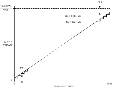 Figure 1. Input / Output Transfer Characteristic
6.9 Typical Characteristics
fSCLK = 20 MHz, TA = 25°C, Input Code Range 48 to 4047, unless otherwise stated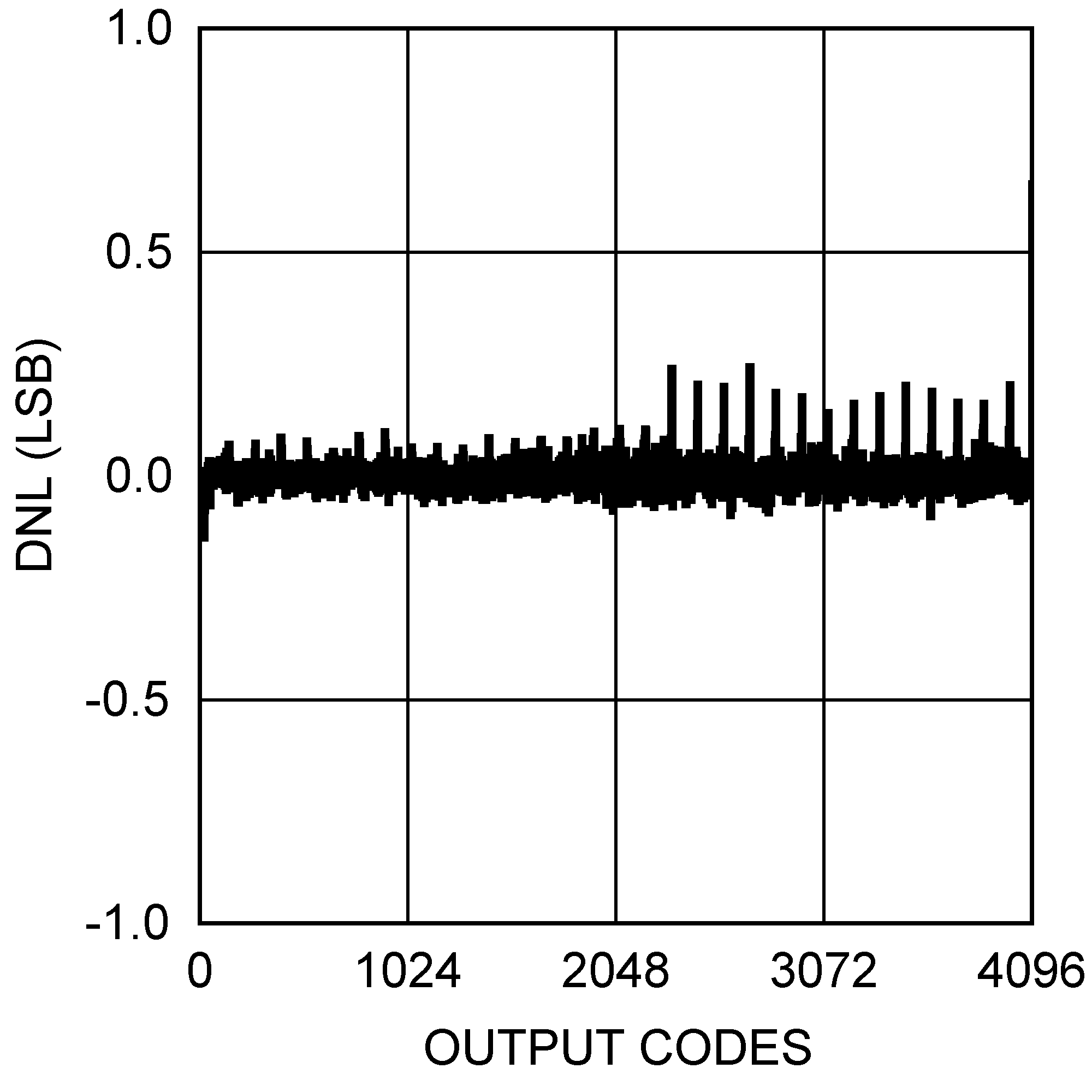 Figure 2. DNL at VA = 2.7 V
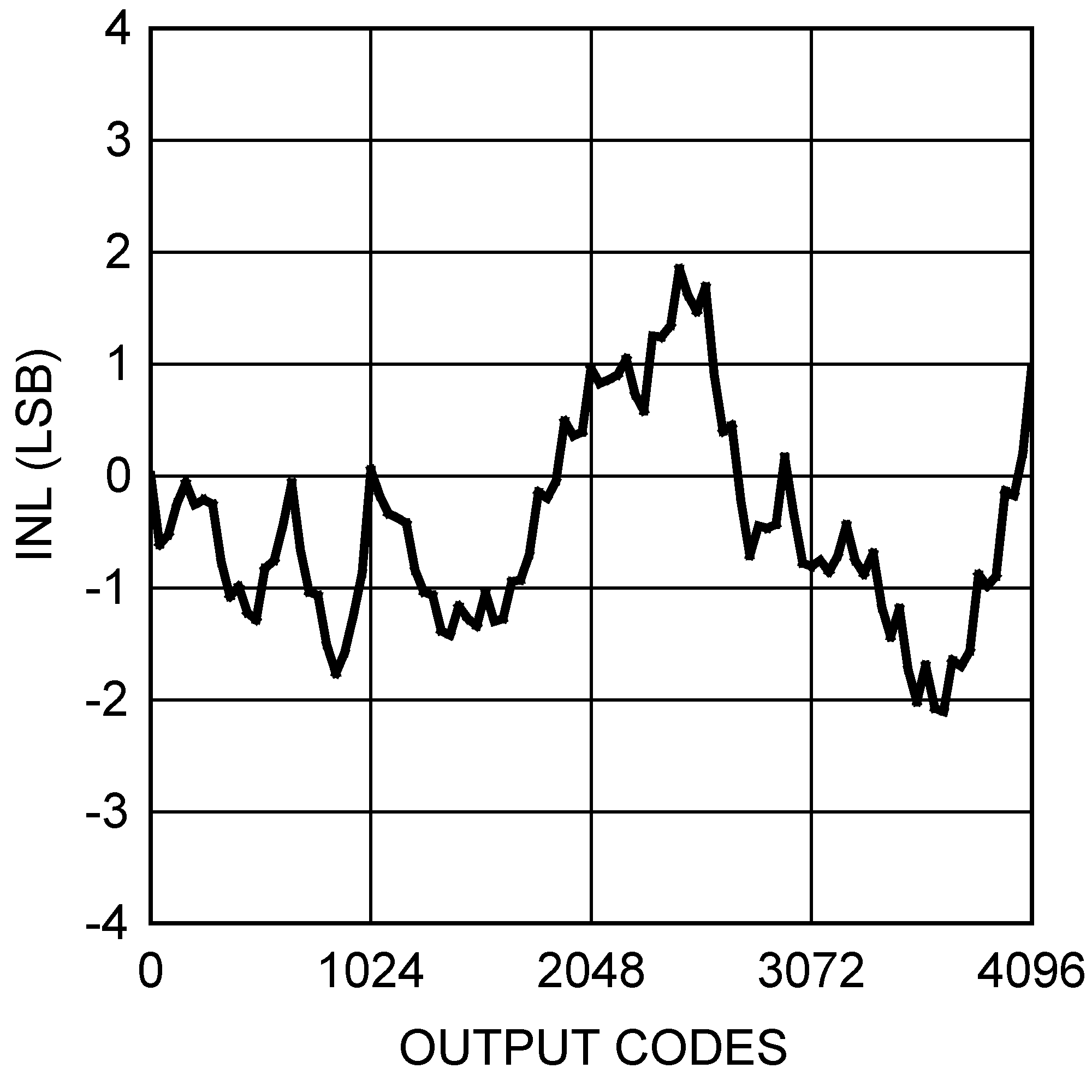 Figure 4. INL at VA = 2.7 V
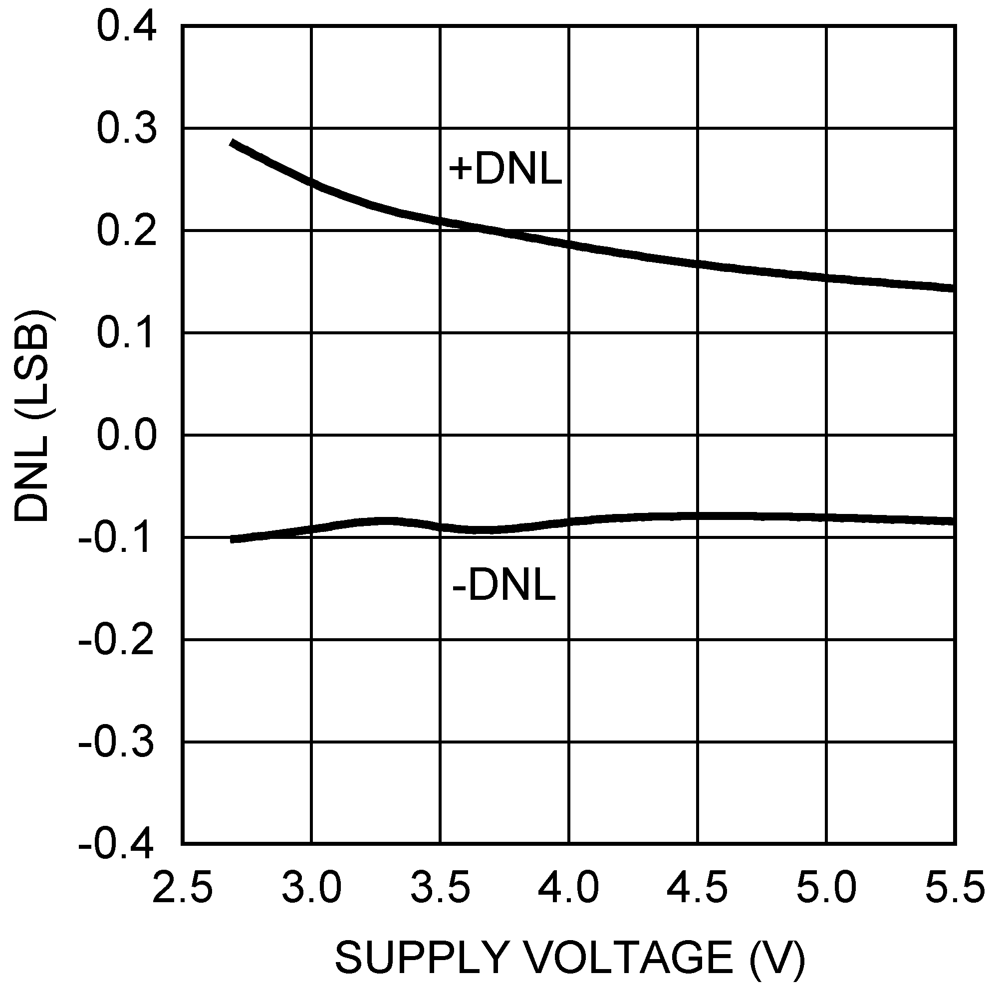 Figure 6. DNL vs VA
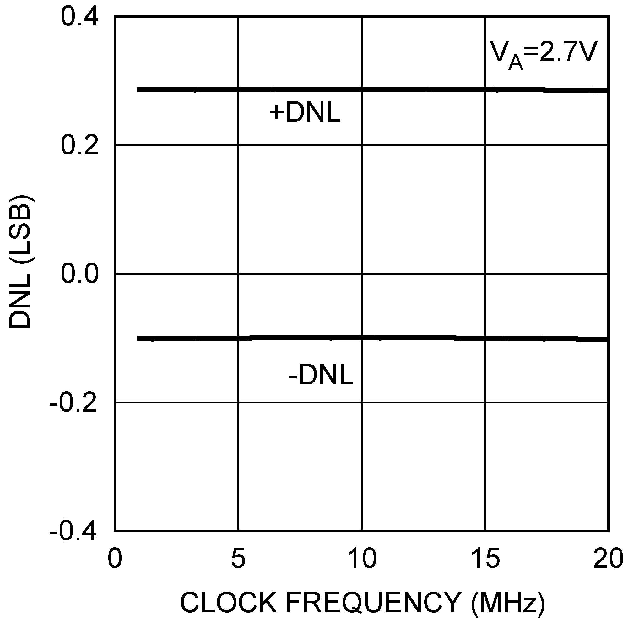 Figure 8. 2.7-V DNL vs fSCLK
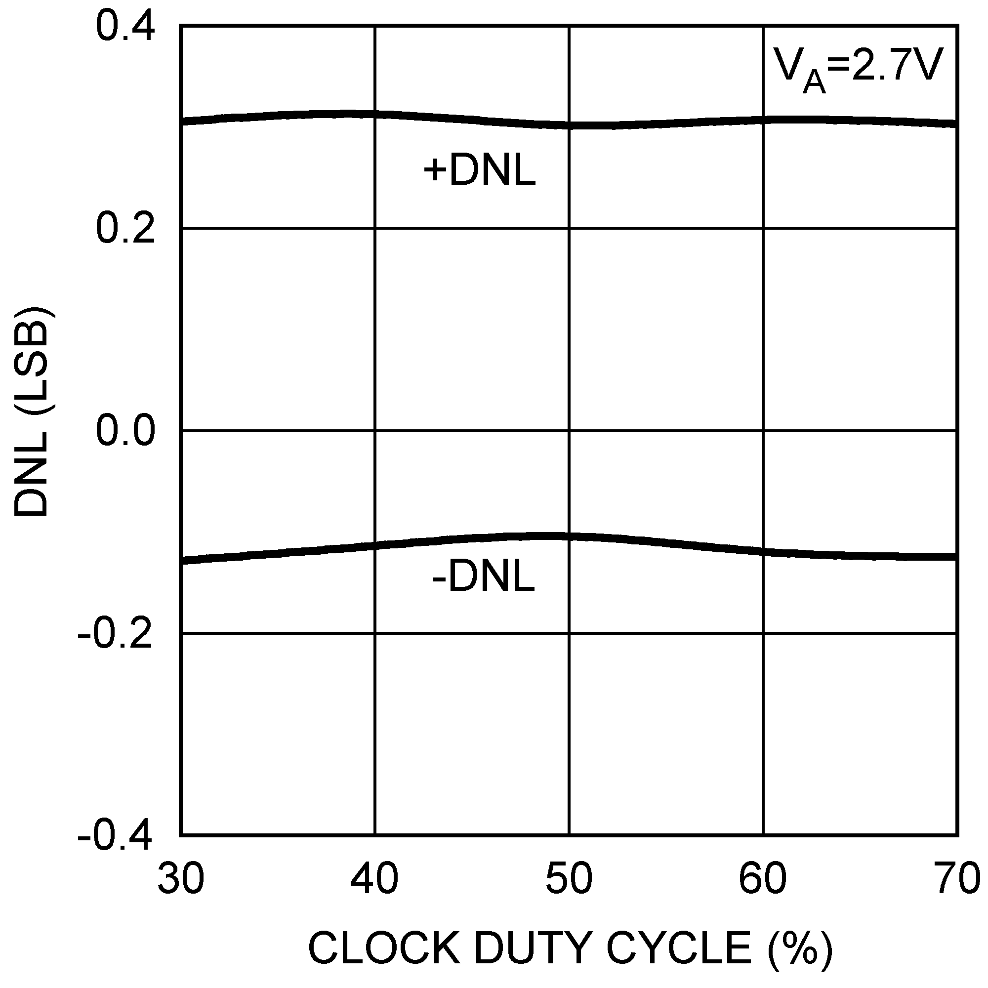 Figure 10. 2.7-V DNL vs Clock Duty Cycle
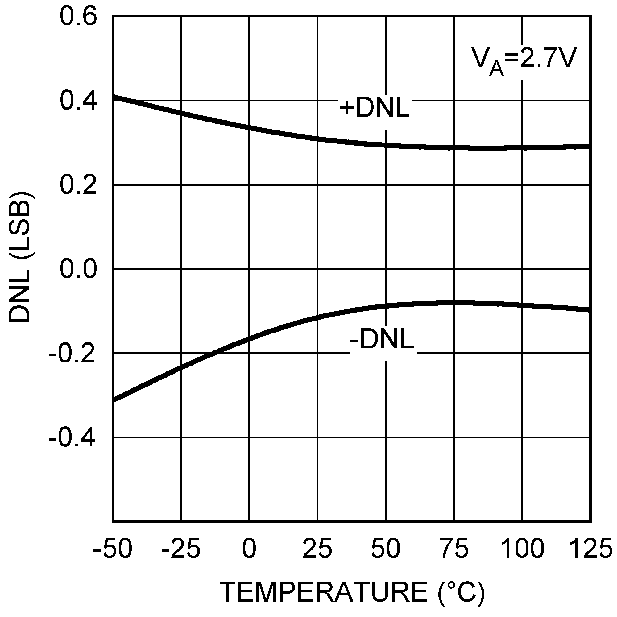 Figure 12. 2.7-V DNL vs Temperature
 Figure 14. 2.7-V INL vs fSCLK
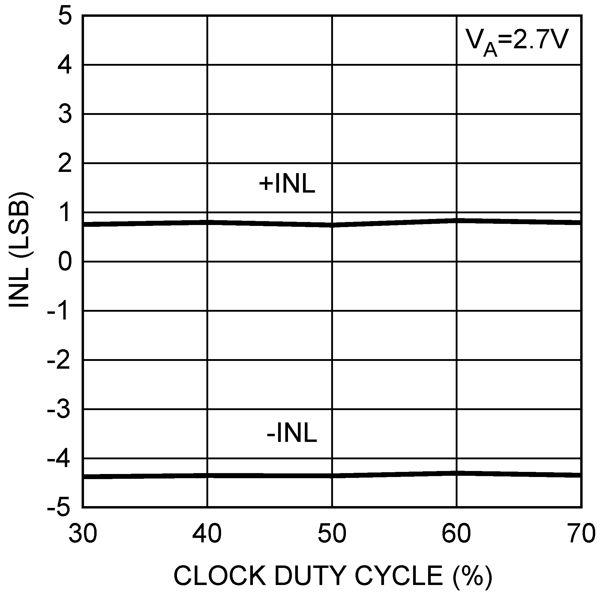 Figure 16. 2.7-V INL vs Clock Duty Cycle
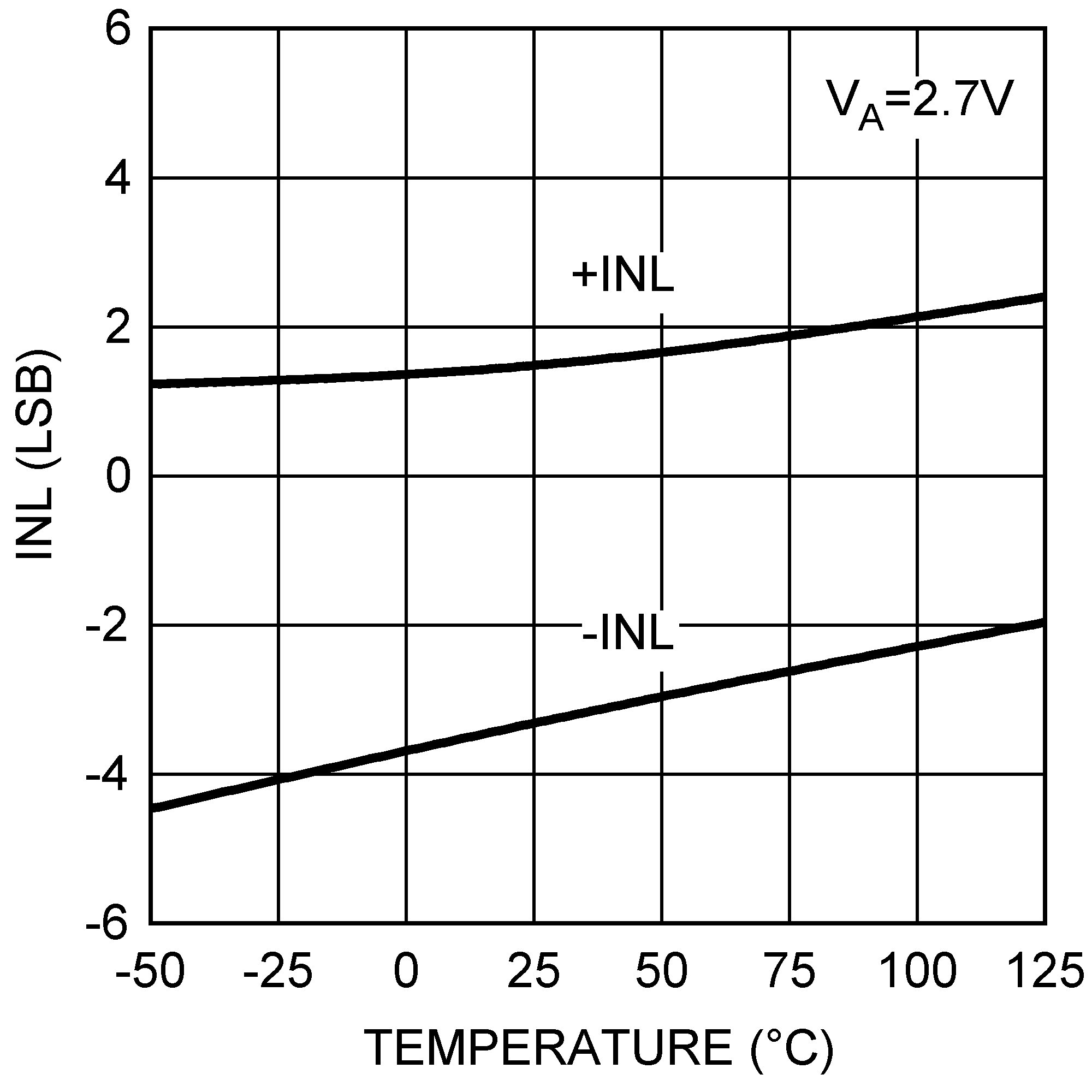 Figure 18. 2.7-V INL vs Temperature
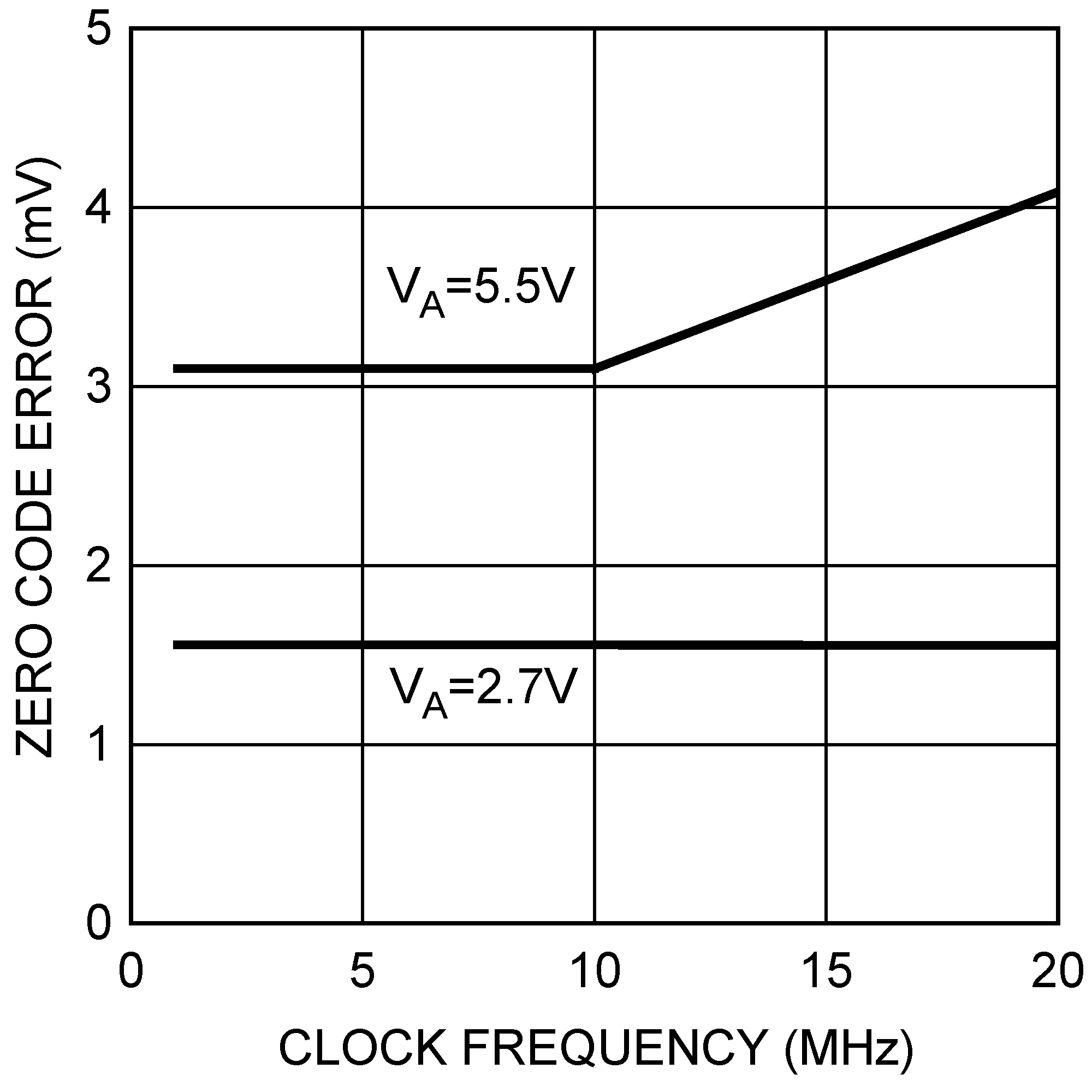 Figure 20. Zero Code Error vs fSCLK
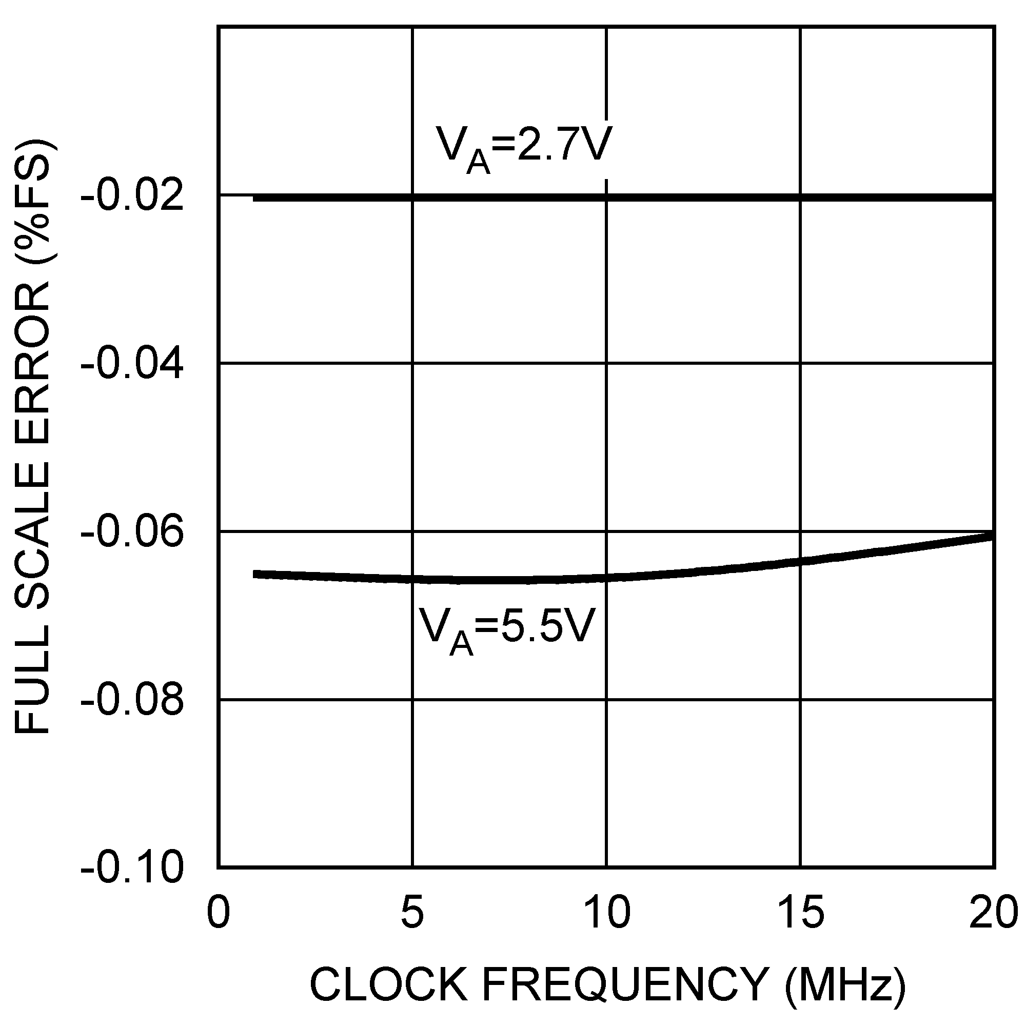 Figure 22. Full-Scale Error vs fSCLK
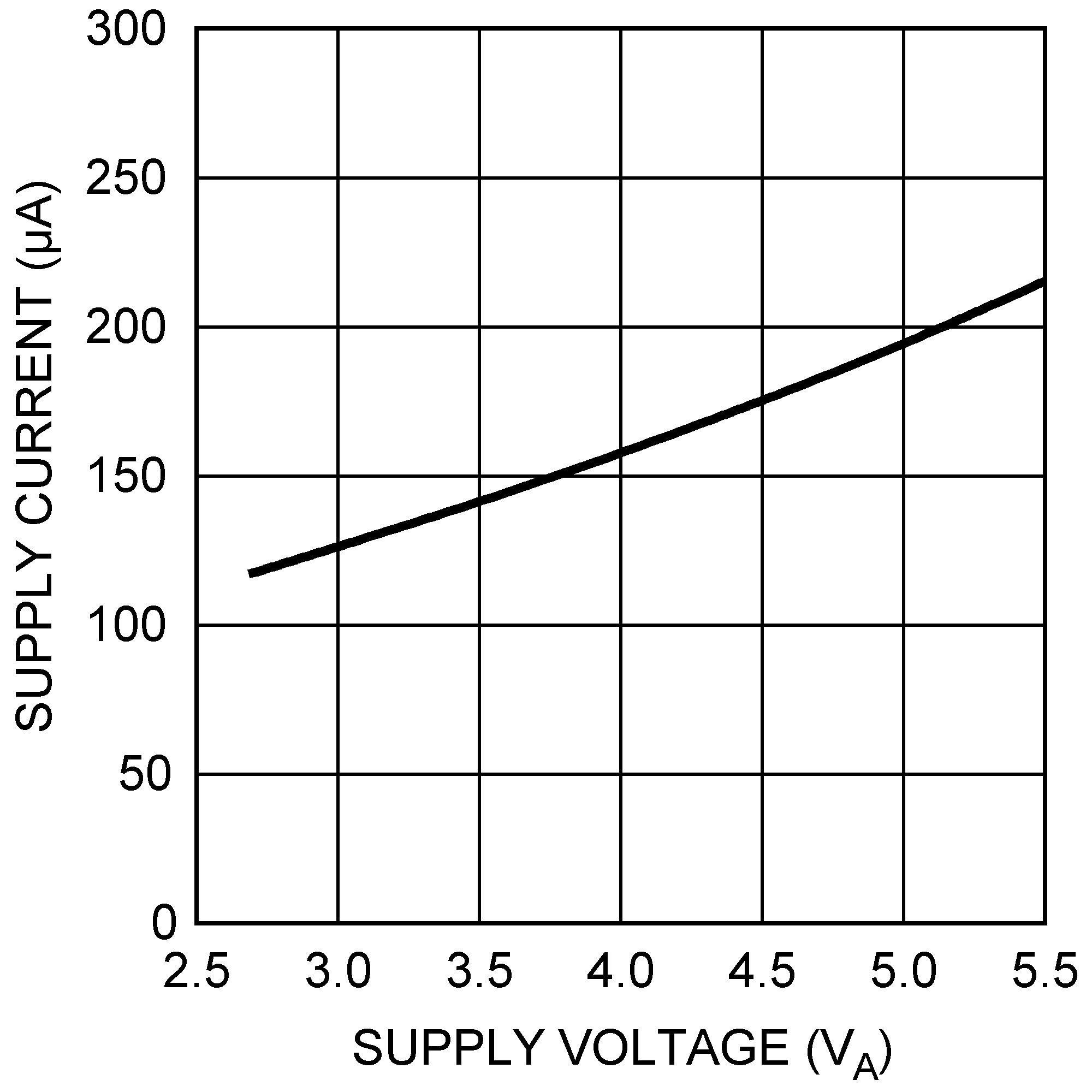 Figure 24. Supply Current vs VA
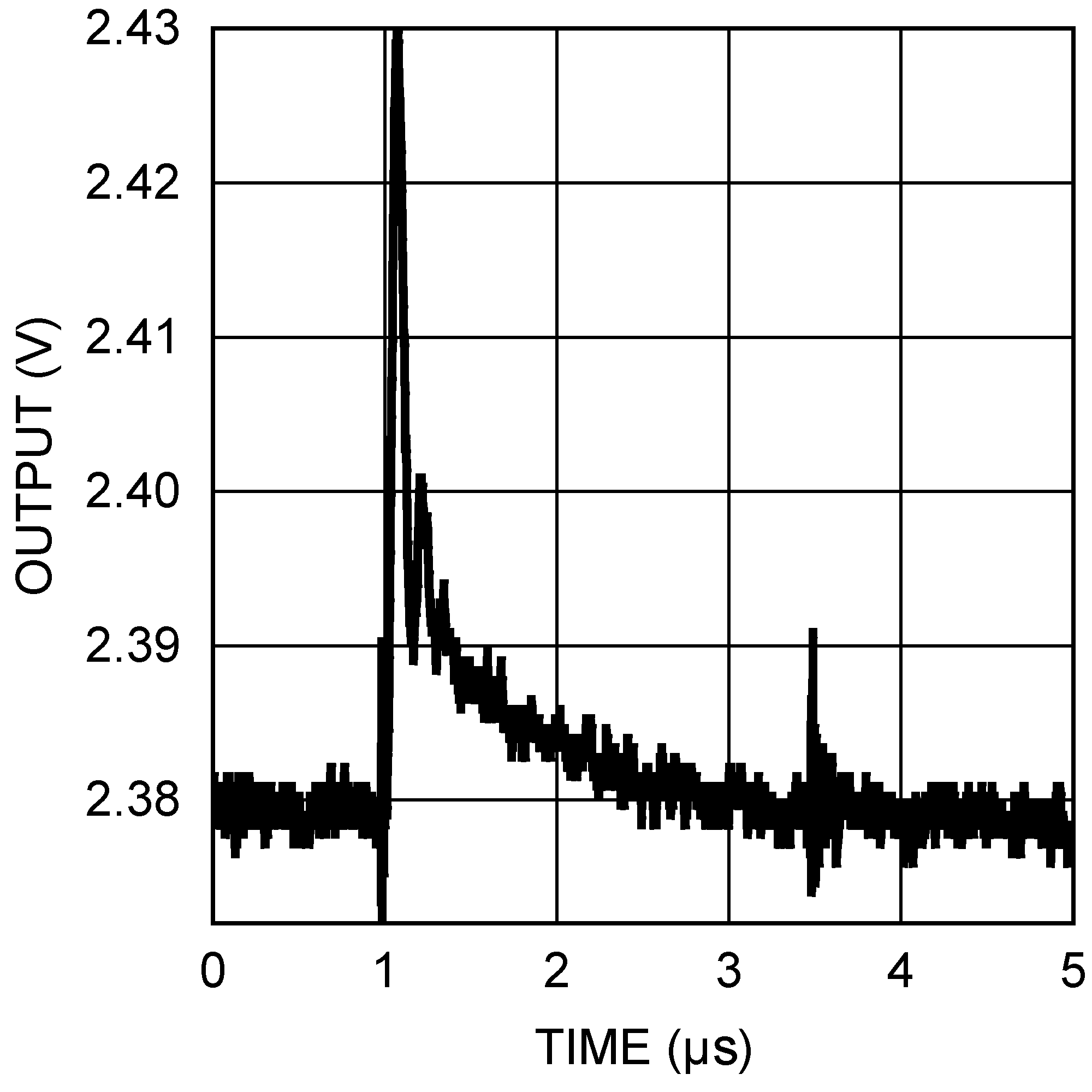 Figure 26. 5-V Glitch Response
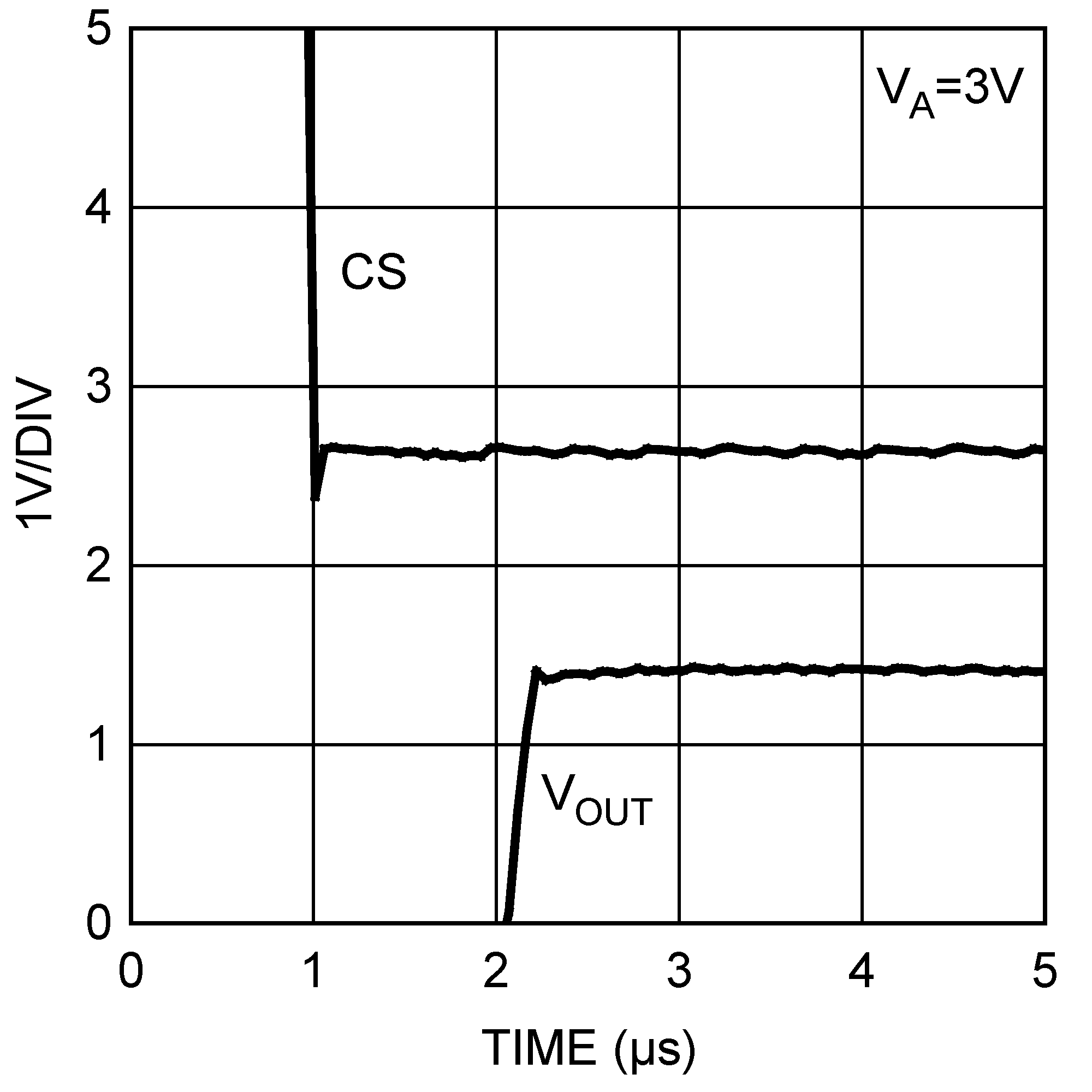 Figure 28. 3-V Wake-Up Time
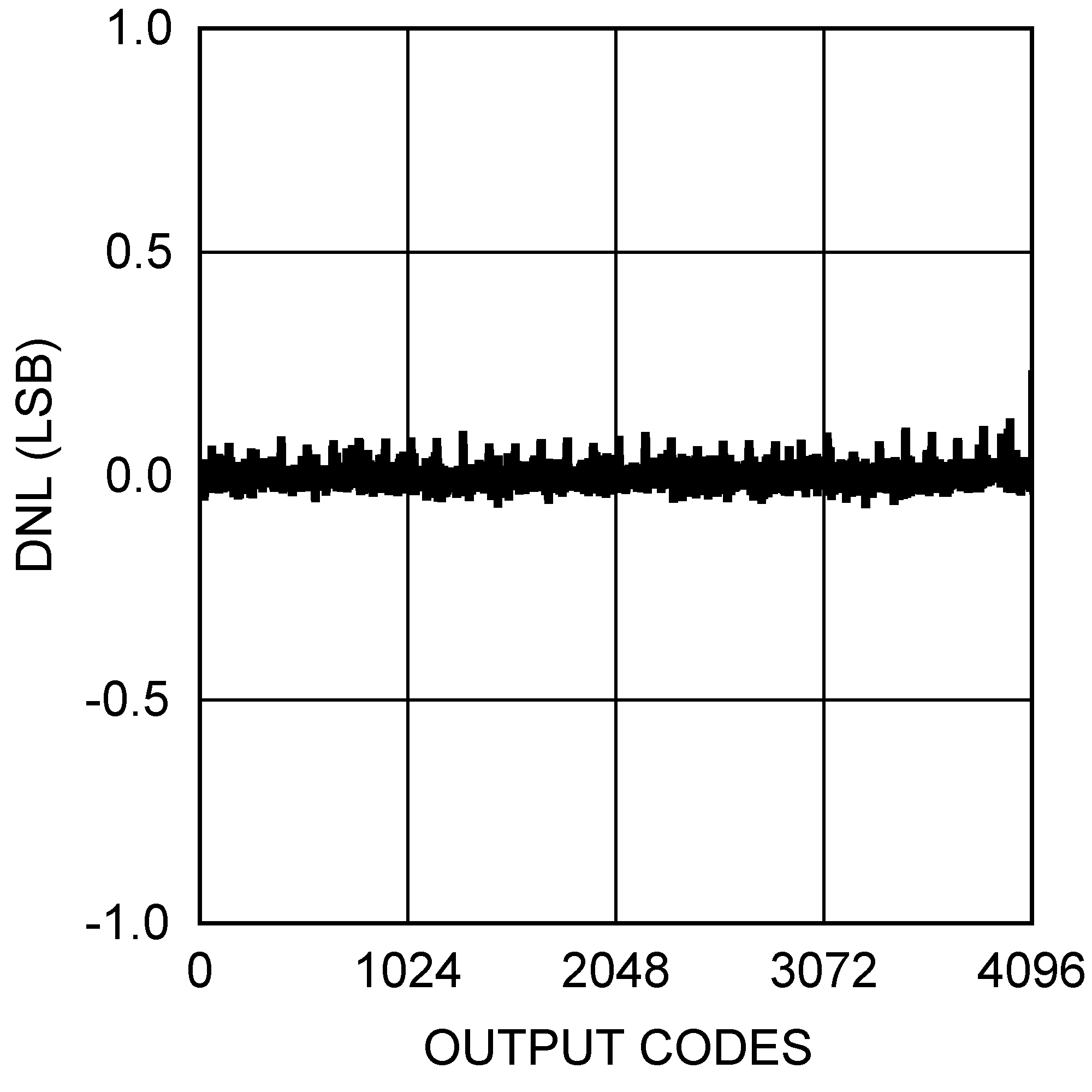 Figure 3. DNL at VA = 5.5 V
 Figure 5. INL at VA = 5.5 V
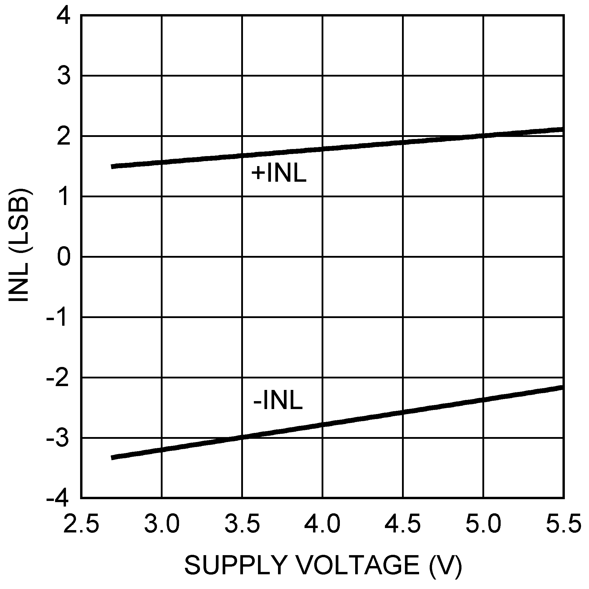 Figure 7. INL vs VA
 Figure 9. 5.5-V DNL vs fSCLK
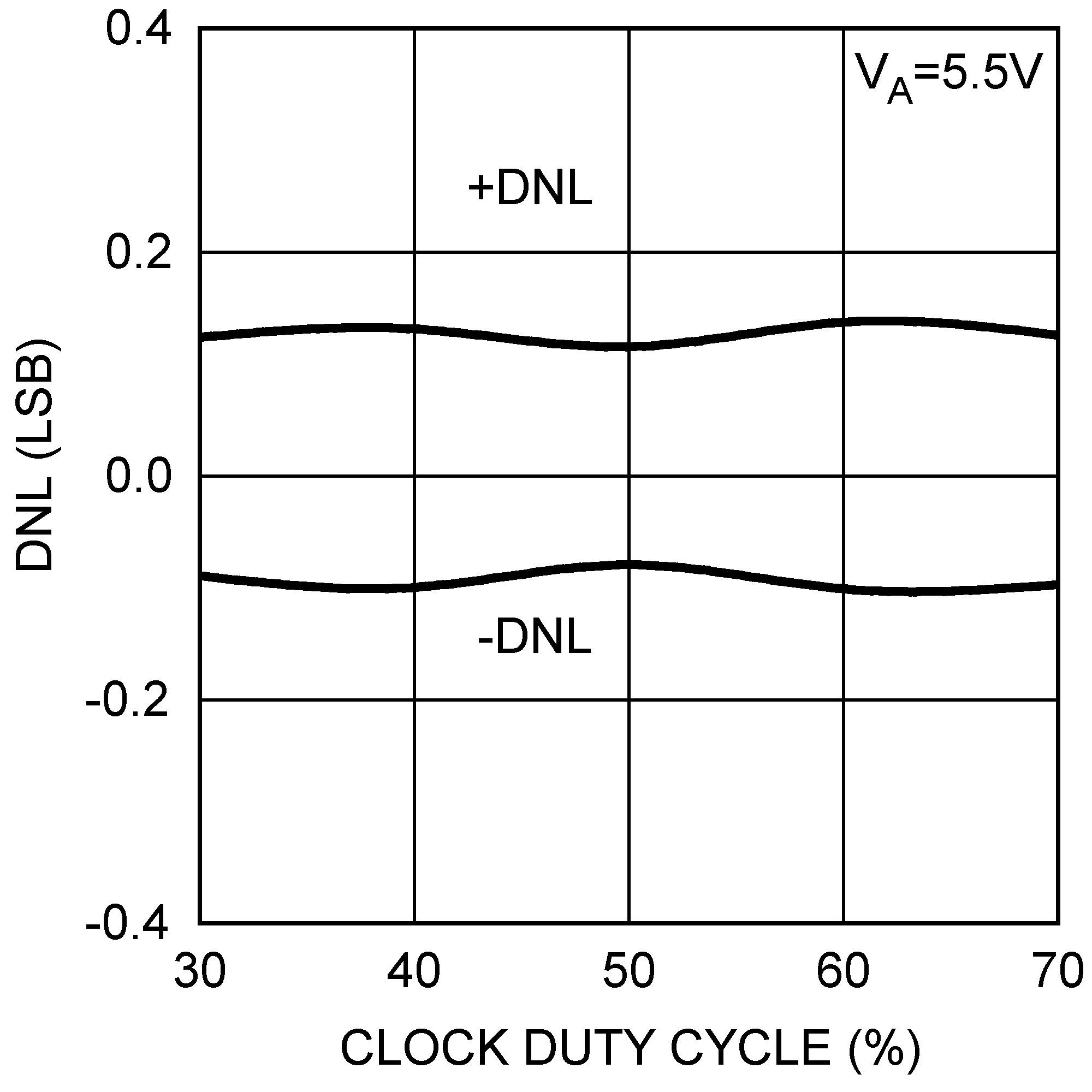 Figure 11. 5.5-V DNL vs Clock Duty Cycle
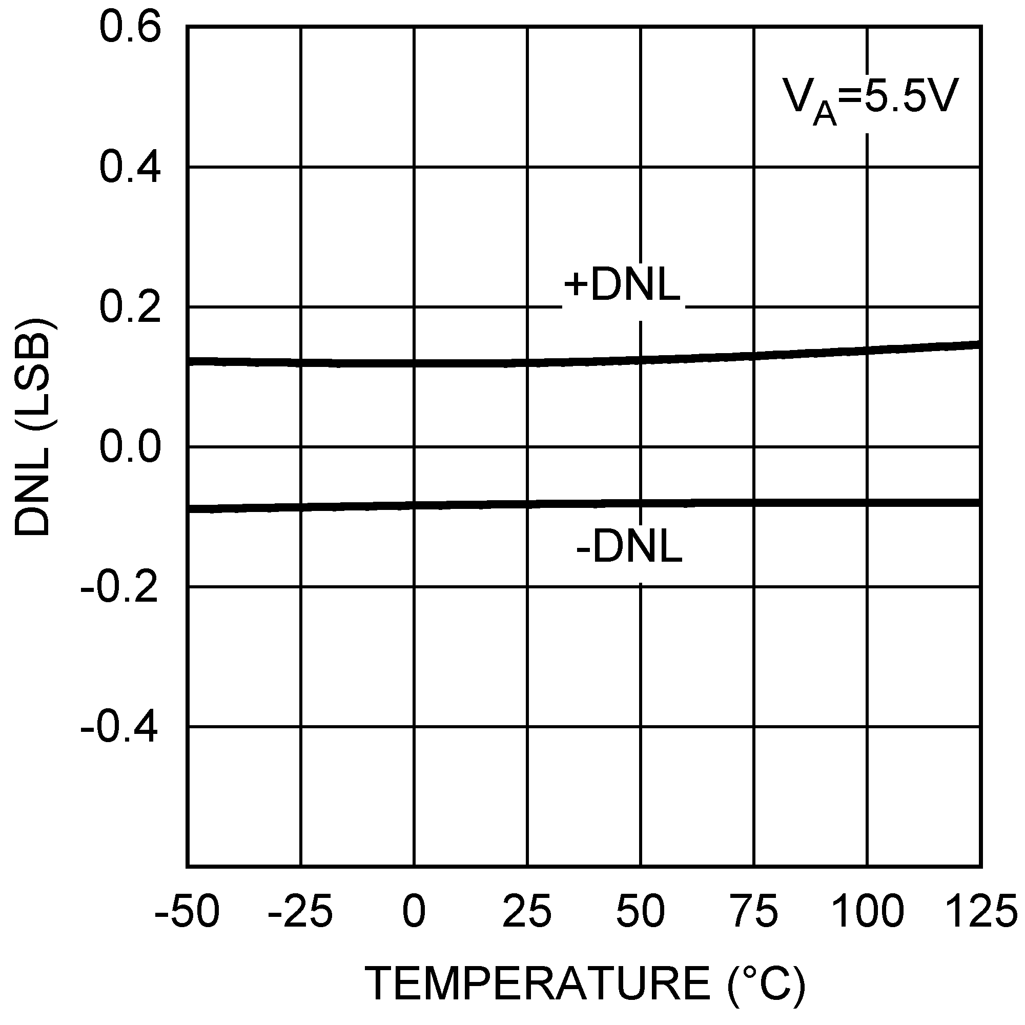 Figure 13. 5.5-V DNL vs Temperature
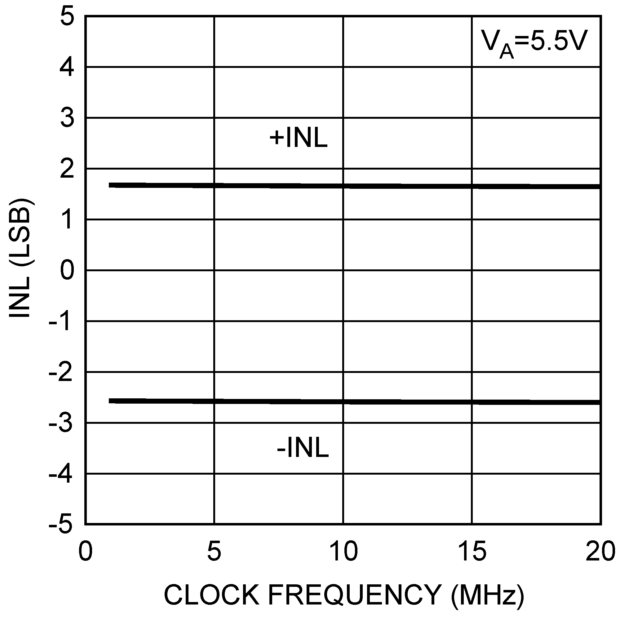 Figure 15. 5.5-V INL vs fSCLK
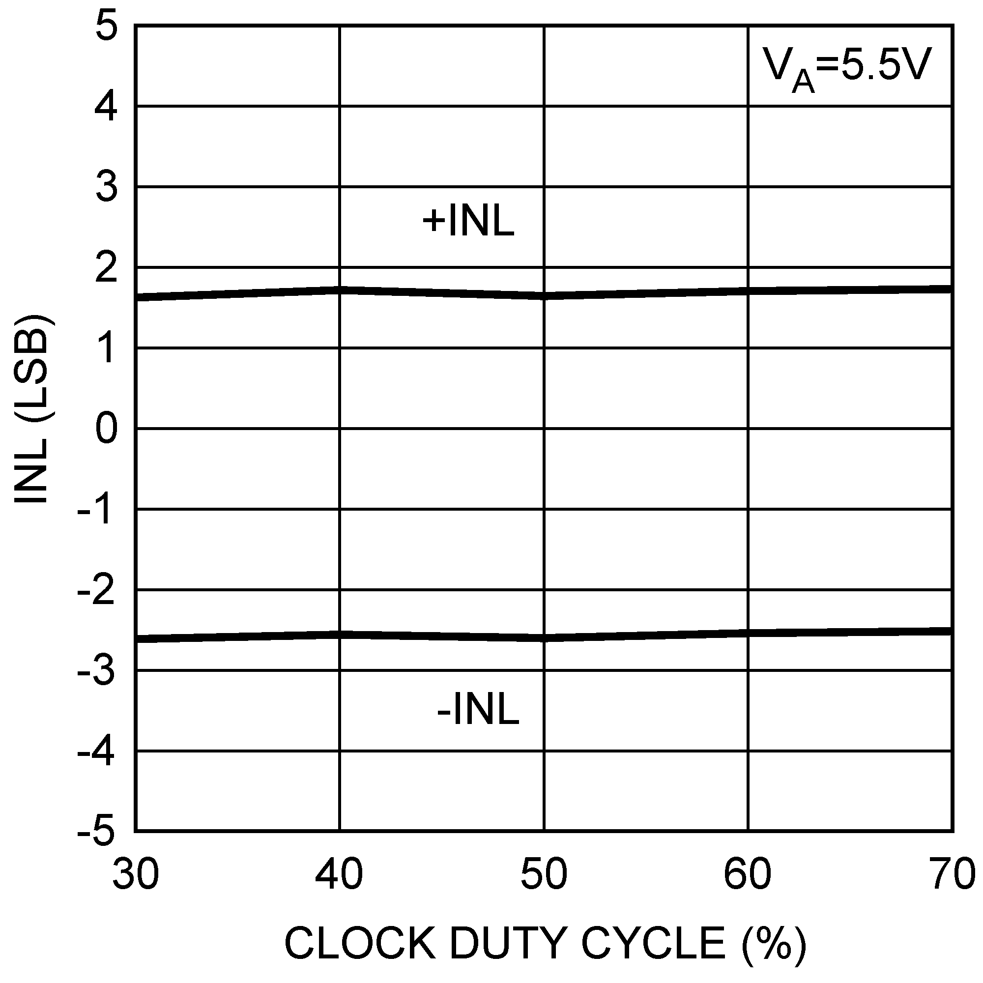 Figure 17. 5.5-V INL vs Clock Duty Cycle
 Figure 19. 5.5-V INL vs Temperature
 Figure 21. Zero Code Error vs Temperature
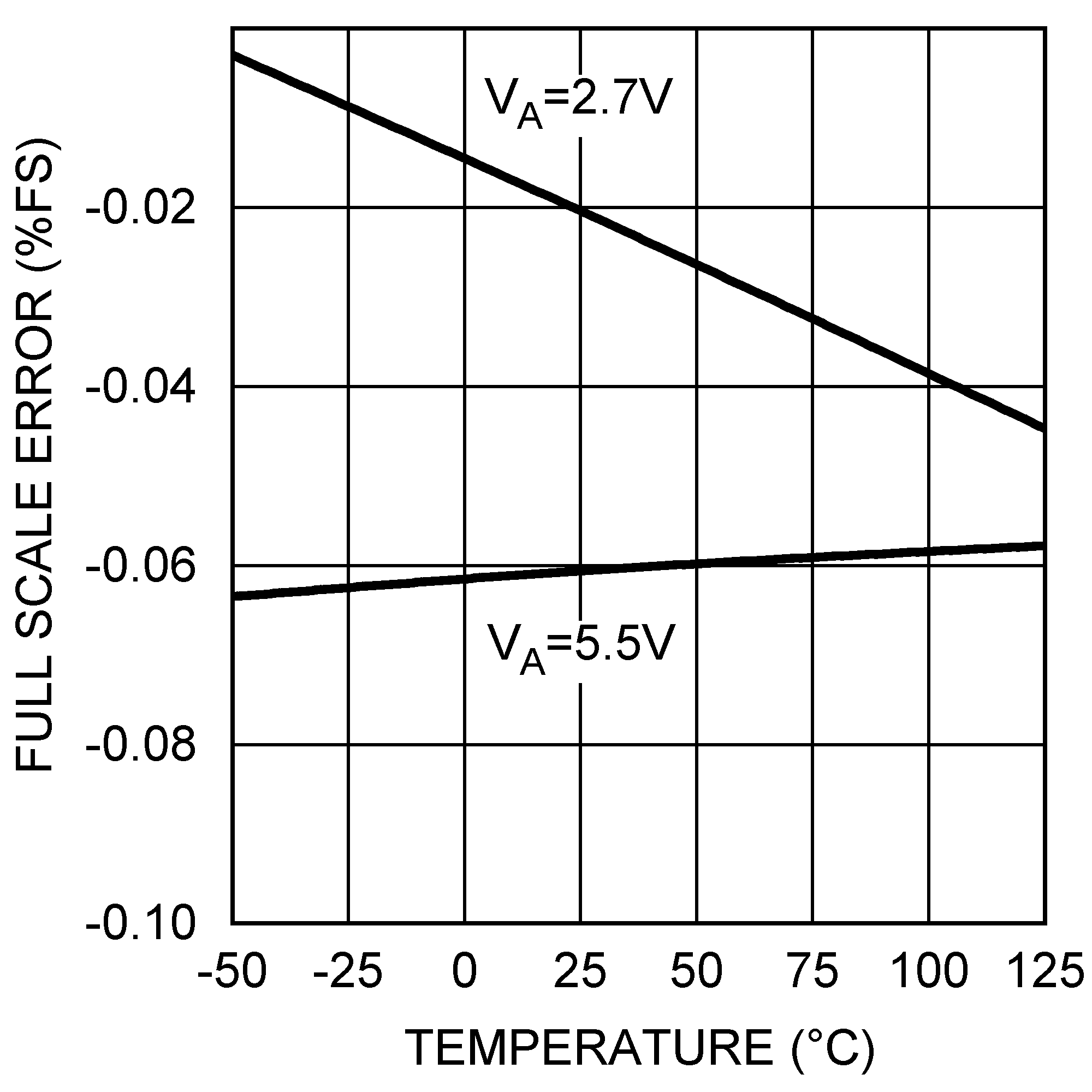 Figure 23. Full-Scale Error vs Temperature
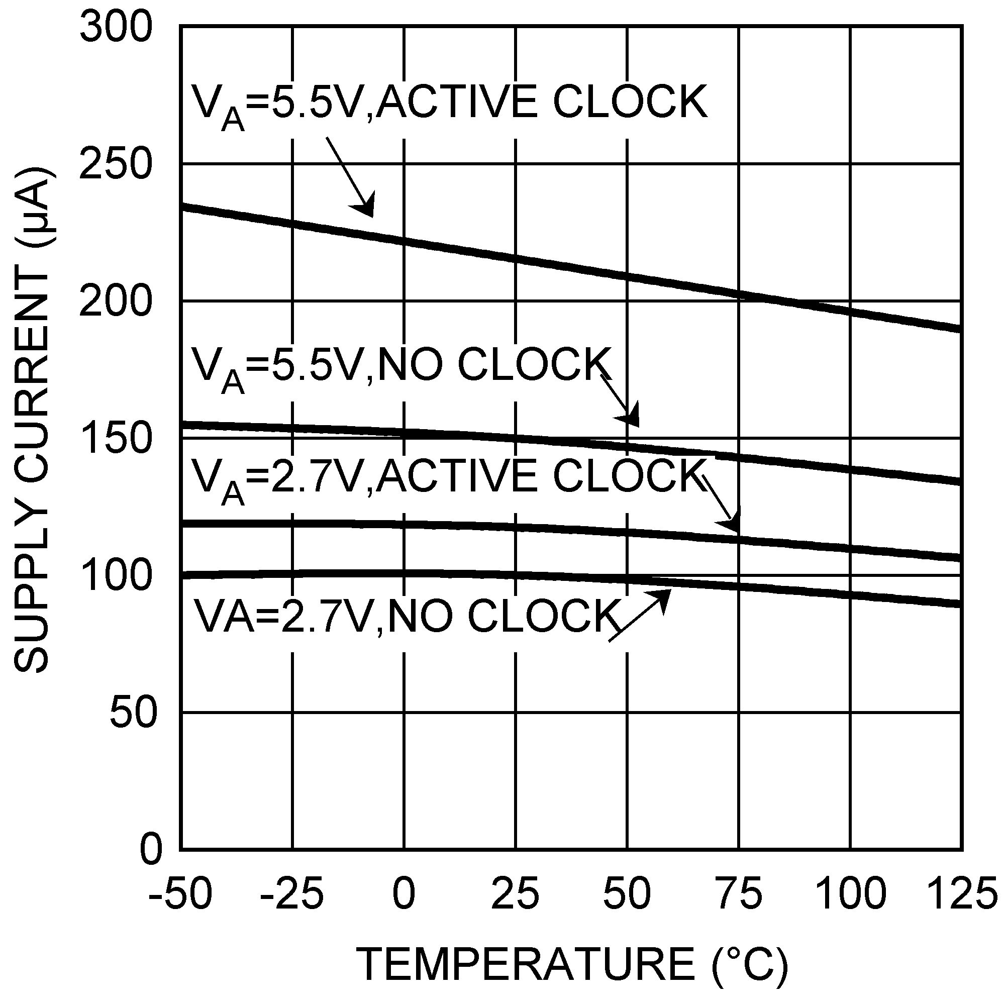 Figure 25. Supply Current vs Temperature
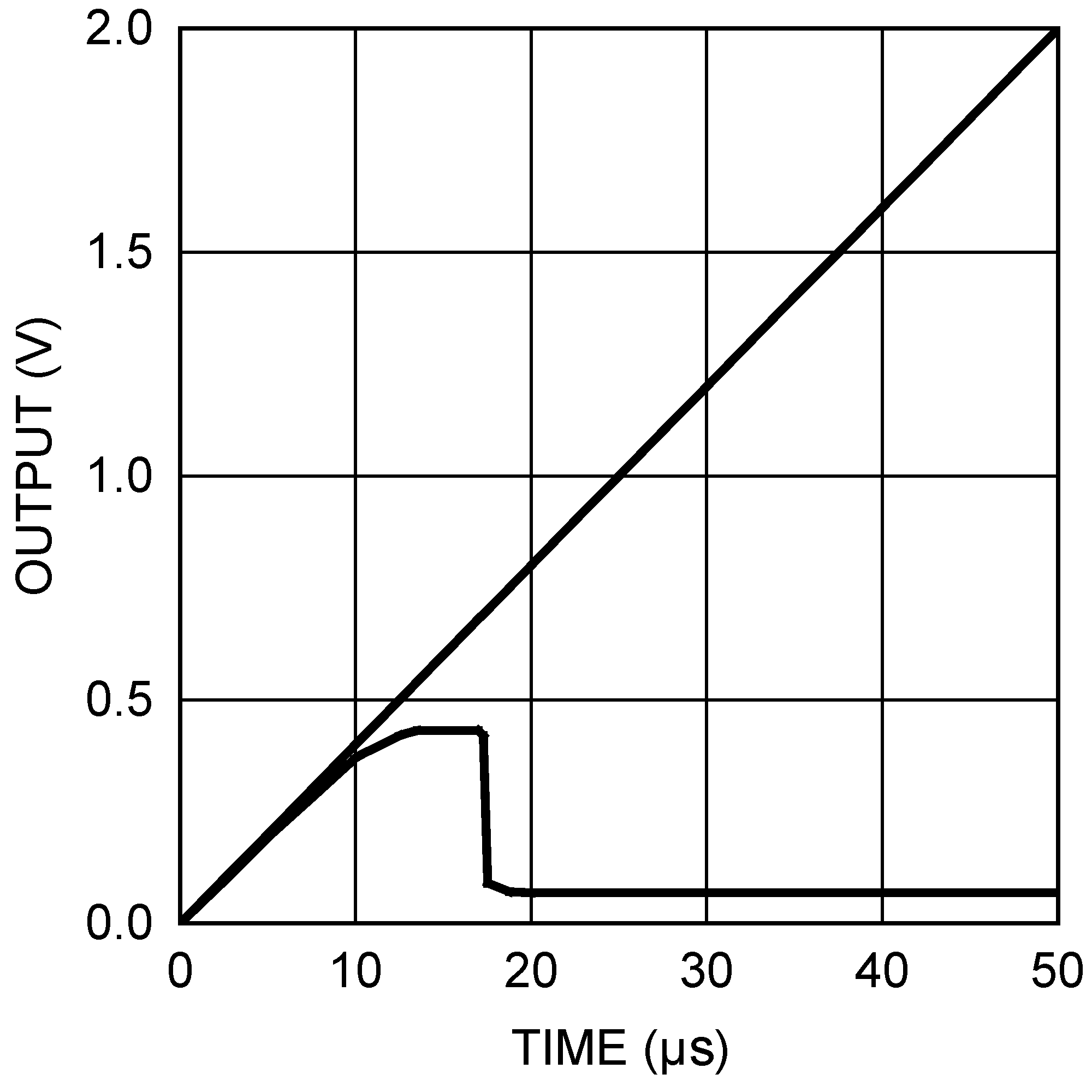 Figure 27. Power-On Reset
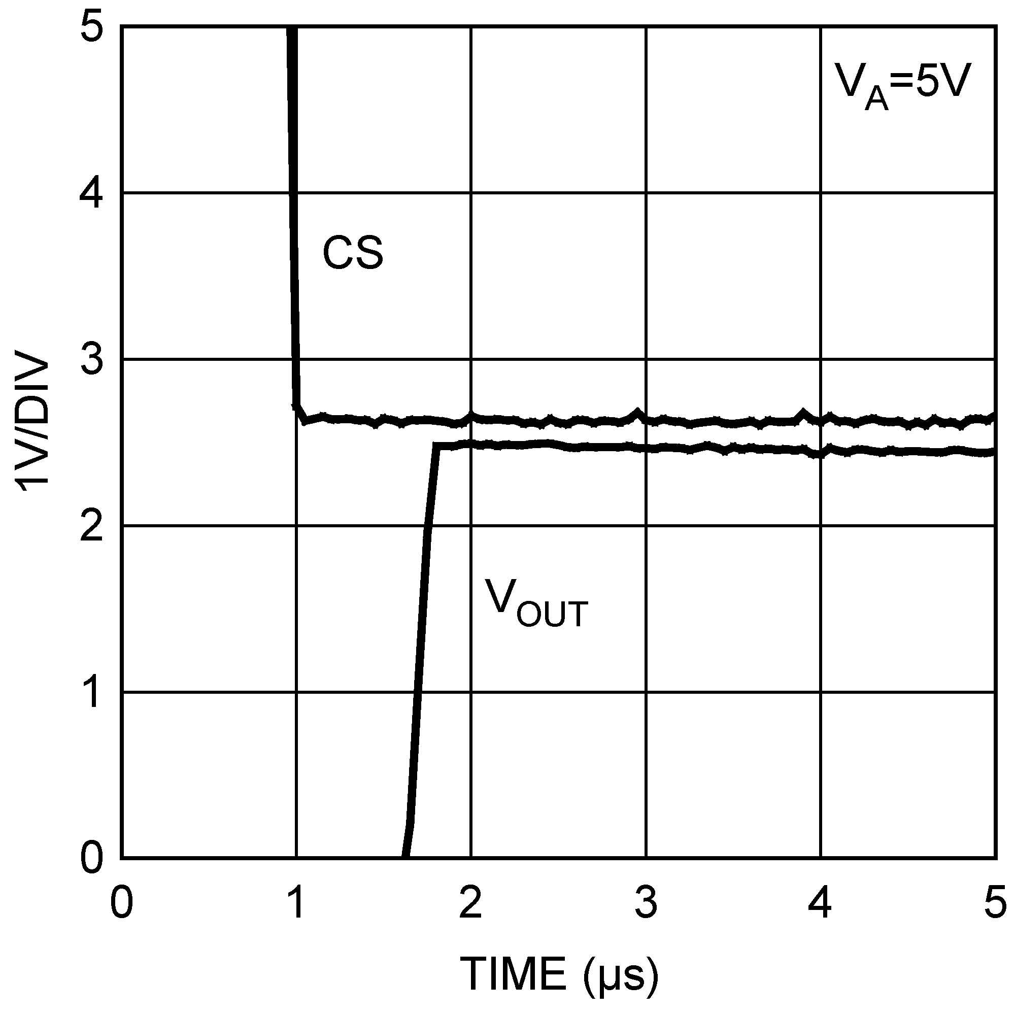 Figure 29. 5-V Wake-Up Time