SLASF48 May 2022 DAC53001 , DAC53002 , DAC63001 , DAC63002
PRODUCTION DATA
- 1 Features
- 2 Applications
- 3 Description
- 4 Revision History
- 5 Pin Configuration and Functions
-
6 Specifications
- 6.1 Absolute Maximum Ratings
- 6.2 ESD Ratings
- 6.3 Recommended Operating Conditions
- 6.4 Thermal Information
- 6.5 Electrical Characteristics: Voltage Output
- 6.6 Electrical Characteristics: Current Output
- 6.7 Electrical Characteristics: Comparator Mode
- 6.8 Electrical Characteristics: General
- 6.9 Timing Requirements: I2C Standard Mode
- 6.10 Timing Requirements: I2C Fast Mode
- 6.11 Timing Requirements: I2C Fast Mode Plus
- 6.12 Timing Requirements: SPI Write Operation
- 6.13 Timing Requirements: SPI Read and Daisy Chain Operation (FSDO = 0)
- 6.14 Timing Requirements: SPI Read and Daisy Chain Operation (FSDO = 1)
- 6.15 Timing Requirements: GPIO
- 6.16 Timing Diagrams
- 6.17 Typical Characteristics: Voltage Output
- 6.18 Typical Characteristics: Current Output
- 6.19 Typical Characteristics: Comparator
- 6.20 Typical Characteristics: General
-
7 Detailed Description
- 7.1 Overview
- 7.2 Functional Block Diagram
- 7.3 Feature Description
- 7.4 Device Functional Modes
- 7.5 Programming
- 7.6
Register Map
- 7.6.1 NOP Register (address = 00h) [reset = 0000h]
- 7.6.2 DAC-X-MARGIN-HIGH Register (address = 13h, 01h) [reset = 0000h]
- 7.6.3 DAC-X-MARGIN-LOW Register (address = 14h, 02h) [reset = 0000h]
- 7.6.4 DAC-X-VOUT-CMP-CONFIG Register (address = 15h, 03h) [reset = 0000h]
- 7.6.5 DAC-X-IOUT-MISC-CONFIG Register (address = 16h, 04h) [reset = 0000h]
- 7.6.6 DAC-X-CMP-MODE-CONFIG Register (address = 17h, 05h) [reset = 0000h]
- 7.6.7 DAC-X-FUNC-CONFIG Register (address = 18h, 06h) [reset = 0000h]
- 7.6.8 DAC-X-DATA Register (address = 1Ch, 19h) [reset = 0000h]
- 7.6.9 COMMON-CONFIG Register (address = 1Fh) [reset = 0FFFh]
- 7.6.10 COMMON-TRIGGER Register (address = 20h) [reset = 0000h]
- 7.6.11 COMMON-DAC-TRIG Register (address = 21h) [reset = 0000h]
- 7.6.12 GENERAL-STATUS Register (address = 22h) [reset = 00h, DEVICE-ID, VERSION-ID]
- 7.6.13 CMP-STATUS Register (address = 23h) [reset = 0000h]
- 7.6.14 GPIO-CONFIG Register (address = 24h) [reset = 0000h]
- 7.6.15 DEVICE-MODE-CONFIG Register (address = 25h) [reset = 0000h]
- 7.6.16 INTERFACE-CONFIG Register (address = 26h) [reset = 0000h]
- 7.6.17 SRAM-CONFIG Register (address = 2Bh) [reset = 0000h]
- 7.6.18 SRAM-DATA Register (address = 2Ch) [reset = 0000h]
- 7.6.19 BRDCAST-DATA Register (address = 50h) [reset = 0000h]
- 7.6.20 PMBUS-PAGE Register [reset = 0300h]
- 7.6.21 PMBUS-OP-CMD-X Register [reset = 0000h]
- 7.6.22 PMBUS-CML Register [reset = 0000h]
- 7.6.23 PMBUS-VERSION Register [reset = 2200h]
- 8 Application and Implementation
- 9 Power Supply Recommendations
- 10Layout
- 11Device and Documentation Support
- 12Mechanical, Packaging, and Orderable Information
Package Options
Mechanical Data (Package|Pins)
- RTE|16
Thermal pad, mechanical data (Package|Pins)
- RTE|16
Orderable Information
3 Description
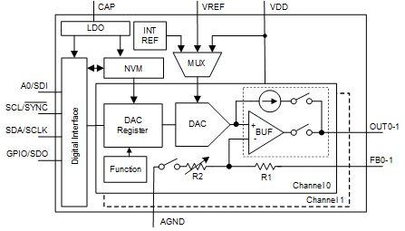
The 12-bit DAC63001 and DAC63002, and the 10‑bit DAC53001 and DAC53002 (collectively referred to as the DACx300x) are a pin-compatible family of ultra-low-power, single-channel and dual-channel, buffered voltage-output and current-output smart digital-to-analog converters (DACs). The DACx300x devices support Hi-Z power-down mode and Hi-Z output during power-off conditions. The DAC outputs provide a force-sense option for use as a programmable comparator and current sink. The multifunction GPIO, function generation, and NVM enable these smart DACs for processor-less applications and design reuse. These devices automatically detect I2C, PMBus, and SPI interfaces and contain an internal reference.
The feature set combined with the tiny package and ultra-low power make these smart DACs an excellent choice for applications such as land mobile radios, pulse oximeters, notebook PCs, and other battery-operated applications for biasing, calibration, and waveform generation.
| PART NUMBER | PACKAGE(1) | BODY SIZE (NOM) |
|---|---|---|
| DACx3001 | WQFN (16) | 3.00 mm x 3.00 mm |
| DACx3002 |
 Simplified Block Diagram