SLASE30 October 2020 DAC43401-Q1 , DAC53401-Q1
PRODUCTION DATA
- 1 Features
- 2 Applications
- 3 Description
- 4 Revision History
- 5 Device Comparison Table
- 6 Pin Configuration and Functions
-
7 Specifications
- 7.1 Absolute Maximum Ratings
- 7.2 ESD Ratings
- 7.3 Recommended Operating Conditions
- 7.4 Thermal Information
- 7.5 Electrical Characteristics
- 7.6 Timing Requirements: I2C Standard Mode
- 7.7 Timing Requirements: I2C Fast Mode
- 7.8 Timing Requirements: I2C Fast Mode Plus
- 7.9 Typical Characteristics: VDD = 1.8 V (Reference = VDD) or VDD = 2 V (Internal Reference)
- 7.10 Typical Characteristics: VDD = 5.5 V (Reference = VDD) or VDD = 5 V (Internal Reference)
- 7.11 Typical Characteristics
-
8 Detailed Description
- 8.1 Overview
- 8.2 Functional Block Diagram
- 8.3 Feature Description
- 8.4 Device Functional Modes
- 8.5 Programming
- 8.6
Register Map
- 8.6.1 STATUS Register (address = D0h) [reset = 000Ch or 0014h]
- 8.6.2 GENERAL_CONFIG Register (address = D1h) [reset = 01F0h]
- 8.6.3 TRIGGER Register (address = D3h) [reset = 0008h]
- 8.6.4 DAC_DATA Register (address = 21h) [reset = 0000h]
- 8.6.5 DAC_MARGIN_HIGH Register (address = 25h) [reset = 0000h]
- 8.6.6 DAC_MARGIN_LOW Register (address = 26h) [reset = 0000h]
- 8.6.7 PMBUS_OPERATION Register (address = 01h) [reset = 0000h]
- 8.6.8 PMBUS_STATUS_BYTE Register (address = 78h) [reset = 0000h]
- 8.6.9 PMBUS_VERSION Register (address = 98h) [reset = 2200h]
- 9 Application and Implementation
- 10Power Supply Recommendations
- 11Layout
- 12Device and Documentation Support
- 13Mechanical, Packaging, and Orderable Information
Package Options
Mechanical Data (Package|Pins)
- DSG|8
Thermal pad, mechanical data (Package|Pins)
- DSG|8
Orderable Information
8.5.1 F/S Mode Protocol
The following steps explain a complete transaction in F/S mode.
- The master initiates data transfer by generating a start condition. The start condition is when a high-to-low transition occurs on the SDA line while SCL is high, as shown in Figure 8-4. All I2C-compatible devices recognize a start condition.
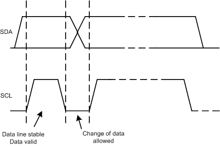
- The master then generates the SCL pulses, and transmits the 7-bit address and the read/write direction bit (R/W) on the SDA line. During all transmissions, the master makes sure that data are valid. A valid data condition requires the SDA line to be stable during the entire high period of the clock pulse, as shown in Figure 8-5. All devices recognize the address sent by the master and compare the address to the respective internal fixed address. Only the slave device with a matching address generates an acknowledge by pulling the SDA line low during the entire high period of the 9th SCL cycle, as shown in Figure 8-3. When the master detects this acknowledge, the communication link with a slave has been established.
- The master generates further SCL cycles to transmit (R/W bit 0) or receive (R/W bit 1) data to the slave. In either case, the receiver must acknowledge the data sent by the transmitter. The acknowledge signal can be generated by the master or by the slave, depending on which is the receiver. The 9-bit valid data sequences consists of 8-data bits and 1 acknowledge-bit, and can continue as long as necessary.
- To signal the end of the data transfer, the master generates a stop condition by pulling the SDA line from low-to-high while the SCL line is high, as shown in Figure 8-4. This action releases the bus and stops the communication link with the addressed slave. All I2C-compatible devices recognize the stop condition. Upon receipt of a stop condition, the bus is released, and all slave devices then wait for a start condition followed by a matching address.
 Figure 8-4 Start and Stop
Conditions
 Figure 8-5 Bit Transfer on the
I2C Bus