SGLS387H July 2007 – August 2016 DAC5675A-SP
PRODUCTION DATA.
- 1 Features
- 2 Applications
- 3 Description
- 4 Revision History
- 5 Description (continued)
- 6 Pin Configuration and Functions
-
7 Specifications
- 7.1 Absolute Maximum Ratings
- 7.2 ESD Ratings
- 7.3 Recommended Operating Conditions
- 7.4 Thermal Information
- 7.5 DC Electrical Characteristics (Unchanged After 100 kRad)
- 7.6 AC Electrical Characteristics (Unchanged After 100 kRad)
- 7.7 Digital Specifications (Unchanged After 100 kRad)
- 7.8 Electrical Characteristics
- 7.9 Typical Characteristics
- 8 Detailed Description
- 9 Application and Implementation
- 10Power Supply Recommendations
- 11Layout
- 12Device and Documentation Support
- 13Mechanical, Packaging, and Orderable Information
Package Options
Refer to the PDF data sheet for device specific package drawings
Mechanical Data (Package|Pins)
- HFG|52
Thermal pad, mechanical data (Package|Pins)
Orderable Information
11 Layout
11.1 Layout Guidelines
- DAC output termination should be placed as close as possible to outputs.
- Keep routing for RBIAS short.
- Decoupling capacitors should be placed as close as possible to supply pins.
- Digital differential inputs must be 50 Ω to ground loosely coupled, or 100-Ω differential tightly coupled.
- Digital differential inputs must be length matched.
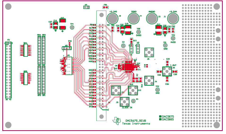
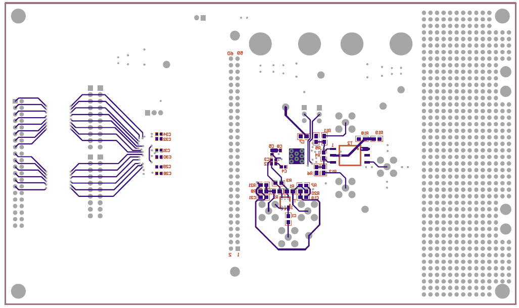
11.2 Layout Example
 Figure 26. Top Layer
 Figure 27. Bottom Layer
11.3 Thermal Considerations
This CQFP package has built-in vias that electrically and thermally connect the bottom of the die to a pad on the bottom of the package. To efficiently remove heat and provide a low-impedance ground path, a thermal land is required on the surface of the PCB directly under the body of the package. During normal surface mount flow solder operations, the heat pad on the underside of the package is soldered to this thermal land creating an efficient thermal path. Normally, the PCB thermal land has a number of thermal vias within it that provide a thermal path to internal copper areas (or to the opposite side of the PCB) that provide for more efficient heat removal. TI typically recommends an 11.9-mm 2-board-mount thermal pad. This allows maximum area for thermal dissipation, while keeping leads away from the pad area to prevent solder bridging. A sufficient quantity of thermal/electrical vias must be included to keep the device within recommended operating conditions. This pad must be electrically ground potential.
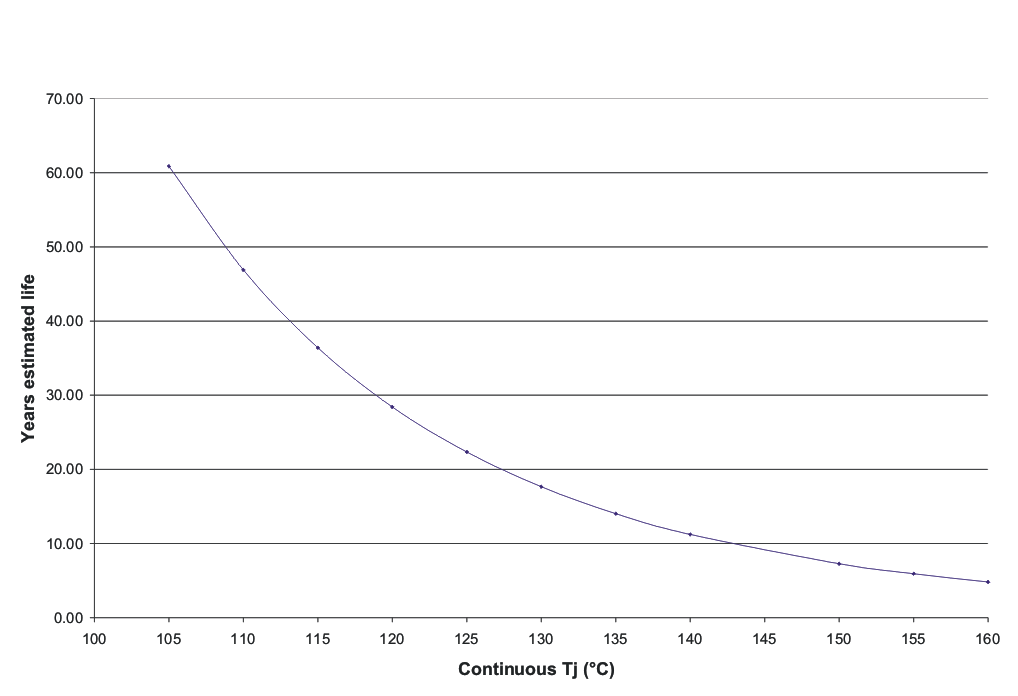
 Figure 28. Estimated Device Life at Elevated Temperatures Electromigration Fail Modes