SGLS387H July 2007 – August 2016 DAC5675A-SP
PRODUCTION DATA.
- 1 Features
- 2 Applications
- 3 Description
- 4 Revision History
- 5 Description (continued)
- 6 Pin Configuration and Functions
-
7 Specifications
- 7.1 Absolute Maximum Ratings
- 7.2 ESD Ratings
- 7.3 Recommended Operating Conditions
- 7.4 Thermal Information
- 7.5 DC Electrical Characteristics (Unchanged After 100 kRad)
- 7.6 AC Electrical Characteristics (Unchanged After 100 kRad)
- 7.7 Digital Specifications (Unchanged After 100 kRad)
- 7.8 Electrical Characteristics
- 7.9 Typical Characteristics
- 8 Detailed Description
- 9 Application and Implementation
- 10Power Supply Recommendations
- 11Layout
- 12Device and Documentation Support
- 13Mechanical, Packaging, and Orderable Information
Package Options
Mechanical Data (Package|Pins)
- HFG|52
Thermal pad, mechanical data (Package|Pins)
Orderable Information
7 Specifications
7.1 Absolute Maximum Ratings
over operating junction temperature range (unless otherwise noted)(1)| MIN | MAX | UNIT | ||
|---|---|---|---|---|
| Supply voltage | AVDD(2) | –0.3 | 3.6 | V |
| DVDD(3) | –0.3 | 3.6 | V | |
| AVDD to DVDD | –0.7 | 0.7 | V | |
| Voltage between AGND and DGND | –0.3 | 0.5 | V | |
| CLK, CLKC(2) | –0.3 | AVDD + 0.3 | V | |
| Digital input D[13:0]A, D[13:0]B(3), SLEEP, DLLOFF | –0.3 | DVDD + 0.3 | V | |
| IOUT1, IOUT2(2) | –1 | AVDD + 0.3 | V | |
| EXTIO, BIASJ(2) | –1 | AVDD + 0.3 | V | |
| Peak input current (any input) | 20 | mA | ||
| Peak total input current (all inputs) | –30 | mA | ||
| Lead temperature 1.6 mm (1/16 inch) from the case for 10 s | 260 | °C | ||
| Storage temperature, Tstg | –65 | 150 | °C | |
(1) Stresses above those listed under Absolute Maximum Ratings may cause permanent damage to the device. Exposure to absolute maximum conditions for extended periods may degrade device reliability. These are stress ratings only, and functional operation of the device at these or any other conditions beyond those indicated under Recommended Operating Conditions is not implied. Exposure to absolute-maximum-rated conditions for extended periods may affect device reliability.
(2) Measured with respect to AGND
(3) Measured with respect to DGND
7.2 ESD Ratings
| VALUE | UNIT | |||
|---|---|---|---|---|
| V(ESD) | Electrostatic discharge | Human body model (HBM), per ANSI/ESDA/JEDEC JS-001, all pins(1) | ±4000 | V |
(1) JEDEC document JEP155 states that 500-V HBM allows safe manufacturing with a standard ESD control process.
7.3 Recommended Operating Conditions
over operating junction temperature range (unless otherwise noted)| MIN | NOM | MAX | UNIT | ||||
|---|---|---|---|---|---|---|---|
| AVDD | Analog supply voltage | 3.15 | 3.3 | 3.6 | V | ||
| DVDD | Digital supply voltage | 3.15 | 3.3 | 3.6 | V | ||
| TJ | Operating junction temperature | 5962-0720401 | –55 | 125 | °C | ||
| 5962-0720402 | –55 | 115 | |||||
7.4 Thermal Information
| THERMAL METRIC(1) | DAC5675A-SP | UNIT | |
|---|---|---|---|
| HFG (CQFP) | |||
| 52 PINS | |||
| RθJA | Junction-to-free-air thermal resistance(2) | 21.813 | °C/W |
| RθJC(bot) | Junction-to-case (bottom) thermal resistance(3) | 0.849 | °C/W |
| RθJB | Junction-to-board thermal resistance | N/A | |
| ψJT | Junction-to-top characterization parameter | N/A | |
| ψJB | Junction-to-board characterization parameter | N/A | |
(1) For more information about traditional and new thermal metrics, see the IC Package Thermal Metrics application report, SPRA953.
(2) Board mounted, per JESD 51-5 methodology
(3) MIL-STD-883 test method 1012
7.5 DC Electrical Characteristics (Unchanged After 100 kRad)
over operating junction temperature range, typical values at 25°C, AVDD = 3.3 V, DVDD = 3.3 V, IO(FS) = 20 mA (unless otherwise noted)| PARAMETER | TEST CONDITIONS | 5962-0720401 | 5962-0720402 | UNIT | |||||
|---|---|---|---|---|---|---|---|---|---|
| MIN | TYP | MAX | MIN | TYP | MAX | ||||
| Resolution | 14 | 14 | bit | ||||||
| DC ACCURACY(1) | |||||||||
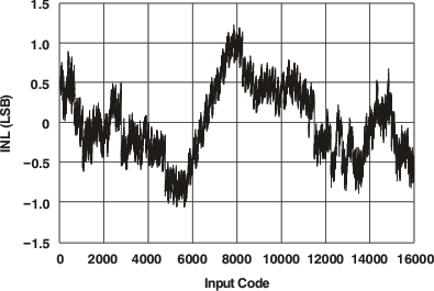
| INL | Integral nonlinearity | TMIN to TMAX | –4 | ±1.5 | 4.6 | –4 | ±1.5 | 4.6 | LSB |
| DNL | Differential nonlinearity | T25°C to TMAX | –2 | ±0.6 | 2.2 | –2 | ±0.6 | 2.2 | LSB |
| TMIN | –2 | ±0.6 | 2.5 | –2 | ±0.6 | 2.5 | LSB | ||
| Monotonicity | Monotonic 12b level | Monotonic 12b level | |||||||
| ANALOG OUTPUT | |||||||||
| IO(FS) | Full-scale output current | 2 | 20 | 2 | 20 | mA | |||
| Output compliance range | AVDD = 3.15 to 3.45 V, IO(FS) = 20 mA |
AVDD – 1 | AVDD + 0.3 | AVDD – 1 | AVDD + 0.3 | V | |||
| Offset error | 0.01 | 0.01 | %FSR | ||||||
| Gain error | Without internal reference | –10 | 5 | 10 | –10 | 5 | 10 | %FSR | |
| With internal reference | –10 | 2.5 | 10 | –10 | 2.5 | 10 | %FSR | ||
| Output resistance | 300 | 300 | kΩ | ||||||
| Output capacitance | 5 | 5 | pF | ||||||
| REFERENCE OUTPUT | |||||||||
| V(EXTIO) | Reference voltage | 1.17 | 1.23 | 1.3 | 1.17 | 1.23 | 1.3 | V | |
| Reference output current(2) | 100 | 100 | nA | ||||||
| REFERENCE INPUT | |||||||||
| V(EXTIO) | Input reference voltage | 0.6 | 1.2 | 1.25 | 0.6 | 1.2 | 1.25 | V | |
| Input resistance | 1 | 1 | MΩ | ||||||
| Small-signal bandwidth | 1.4 | 1.4 | MHz | ||||||
| Input capacitance | 100 | 100 | pF | ||||||
| TEMPERATURE COEFFICIENTS | |||||||||
| Offset drift | 12 | 12 | ppm of FSR/°C | ||||||
| ΔV(EXTIO) | Reference voltage drift | ±50 | ±50 | ppm/°C | |||||
| POWER SUPPLY | |||||||||
| AVDD | Analog supply voltage | 3.15 | 3.3 | 3.6 | 3.15 | 3.3 | 3.6 | V | |
| DVDD | Digital supply voltage | 3.15 | 3.3 | 3.6 | 3.15 | 3.3 | 3.6 | V | |
| I(AVDD) | Analog supply current(3) | 115 | 148 | 115 | 138 | mA | |||
| I(DVDD) | Digital supply current(3) | 85 | 130 | 85 | 120 | mA | |||
| PD | Power dissipation | Sleep mode | 18 | 18 | mW | ||||
| AVDD = 3.3 V, DVDD = 3.3 V | 660 | 900 | 660 | 850 | mW | ||||
| APSRR | Analog and digital power-supply rejection ratio | AVDD = 3.15 to 3.45 V | –0.9 | ±0.1 | 0.9 | –0.9 | ±0.1 | 0.9 | %FSR/V |
| DPSRR | –0.9 | ±0.1 | 0.9 | –0.9 | ±0.1 | 0.9 | |||
(1) Measured differential at IOUT1 and IOUT2: 25 Ω to AVDD.
(2) Use an external buffer amplifier with high impedance input to drive any external load.
(3) Measured at ƒCLK = 400 MSPS and ƒOUT = 70 MHz.
7.6 AC Electrical Characteristics (Unchanged After 100 kRad)
over operating junction temperature range, typical values at 25°C, AVDD = 3.3 V, DVDD = 3.3 V, IO(FS) = 20 mA, differential transformer-coupled output, 50-Ω doubly-terminated load (unless otherwise noted)| PARAMETER | TEST CONDITIONS | 5962-0720401 | 5962-0720402 | UNIT | ||||||
|---|---|---|---|---|---|---|---|---|---|---|
| MIN | TYP | MAX | MIN | TYP | MAX | |||||
| ANALOG OUTPUT | ||||||||||
| ƒCLK | Output update rate | 400 | 400 | MSPS | ||||||
| ts(DAC) | Output setting time to 0.1% | Transition: code x2000 to x23FF | 12 | 12 | ns | |||||
| tPD | Output propagation delay | 1 | 1 | ns | ||||||
| tr(IOUT) | Output rise time, 10% to 90% | 300 | 300 | ps | ||||||
| tf(IOUT) | Output fall time, 90% to 10% | 300 | 300 | ps | ||||||
| Output noise | IOUTFS = 20 mA | 55 | 55 | pA/√Hz | ||||||
| IOUTFS = 2 mA | 30 | 30 | ||||||||
| AC LINEARITY | ||||||||||
| THD | Total harmonic distortion | ƒCLK = 100 MSPS, ƒOUT = 19.9 MHz | 70 | 70 | dBc | |||||
| ƒCLK = 160 MSPS, ƒOUT = 41 MHz | 72 | 72 | ||||||||
| ƒCLK = 200 MSPS, ƒOUT = 70 MHz | 68 | 68 | ||||||||
| ƒCLK = 400 MSPS |
ƒOUT = 20 MHz | 60 | 68 | 62 | 68 | |||||
| ƒOUT = 20 MHz, for TMIN | 57 | 57 | ||||||||
| ƒOUT = 70 MHz | 67 | 67 | ||||||||
| ƒOUT = 140 MHz | 55 | 55 | ||||||||
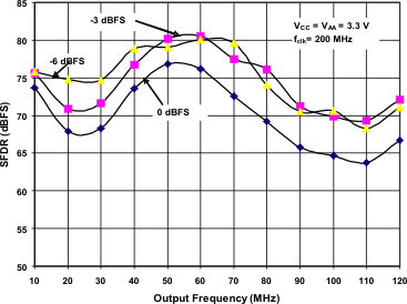
| SFDR | Spurious-free dynamic range to Nyquist | ƒCLK = 100 MSPS, ƒOUT = 19.9 MHz | 70 | 70 | dBc | |||||
| ƒCLK = 160 MSPS, ƒOUT = 41 MHz | 73 | 73 | ||||||||
| ƒCLK = 200 MSPS, ƒOUT = 70 MHz | 70 | 70 | ||||||||
| ƒCLK = 400 MSPS |
ƒOUT = 20 MHz | 62 | 68 | 63 | 68 | |||||
| ƒOUT = 20 MHz, for TMIN | 61 | 61 | ||||||||
| ƒOUT = 70 MHz | 69 | 69 | ||||||||
| ƒOUT = 140 MHz | 56 | 56 | ||||||||
| SFDR | Spurious-free dynamic range within a window, 5 MHz span | ƒCLK = 100 MSPS, ƒOUT = 19.9 MHz | 82 | 82 | dBc | |||||
| ƒCLK = 160 MSPS, ƒOUT = 41 MHz | 77 | 77 | ||||||||
| ƒCLK = 200 MSPS, ƒOUT = 70 MHz | 82 | 82 | ||||||||
| ƒCLK = 400 MSPS |
ƒOUT = 20 MHz | 82 | 82 | |||||||
| ƒOUT = 70 MHz | 82 | 82 | ||||||||
| ƒOUT = 140 MHz | 75 | 75 | ||||||||
| SNR | Signal-to-noise ratio | ƒCLK = 400 MSPS, ƒOUT = 20 MHz | 60 | 67 | 60 | 67 | dBc | |||
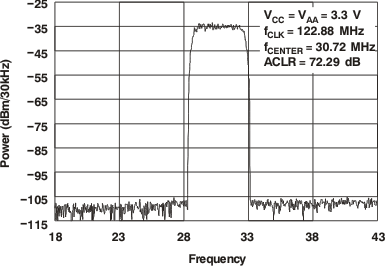
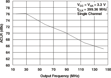
| ACPR | Adjacent channel power ratio WCDM A with 3.84 MHz BW, 5 MHz channel spacing | ƒCLK = 122.88 MSPS, IF = 30.72 MHz, see Figure 9 | 73 | 73 | dB | |||||
| ƒCLK = 245.76 MSPS, IF = 61.44 MHz, | 71 | 71 | ||||||||
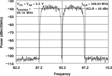
| ƒCLK = 399.36 MSPS, IF = 153.36 MHz, see Figure 11 | 65 | 65 | ||||||||
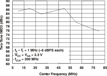
| IMD | Two-tone intermodulation to Nyquist (each tone at –6 dBfs) |
ƒCLK = 400 MSPS, ƒOUT1 = 70 MHz, ƒOUT2 = 71 MHz | 73 | 73 | dBc | |||||
| ƒCLK = 400 MSPS, ƒOUT1 = 140 MHz, ƒOUT2 = 141 MHz | 62 | 62 | ||||||||
| Four-tone intermodulation, 15-MHz span, missing center tone (each tone at –16 dBfs) | ƒCLK = 156 MSPS, ƒOUT = 15.6, 15.8, 16.2, 16.4 MHz | 82 | 82 | |||||||
| ƒCLK = 400 MSPS, ƒOUT = 68.1, 69.3, 71.2, 72 MHz | 74 | 74 | ||||||||
7.7 Digital Specifications (Unchanged After 100 kRad)
over operating junction temperature range, typical values at 25°C, AVDD = 3.3 V, DVDD = 3.3 V (unless otherwise noted)| PARAMETER | TEST CONDITIONS | 5962-0720401 | 5962-0720402 | UNIT | |||||
|---|---|---|---|---|---|---|---|---|---|
| MIN | TYP | MAX | MIN | TYP | MAX | ||||
| LVDS INTERFACE: NODES D[13:0]A, D[13:0]B | |||||||||
| VITH+ | Positive-going differential input voltage threshold | 100 | 100 | mV | |||||
| VITH– | Negative-going differential input voltage threshold | –100 | –100 | mV | |||||
| ZT | Internal termination impedance | 90 | 110 | 132 | 90 | 110 | 132 | Ω | |
| CI | Input capacitance | 2 | 2 | pF | |||||
| CMOS INTERFACE (SLEEP) | |||||||||
| VIH | High-level input voltage | 2 | 3.3 | 2 | 3.3 | V | |||
| VIL | Low-level input voltage | 0 | 0.8 | 0 | 0.8 | V | |||
| IIH | High-level input current | 10 | 100 | 10 | 100 | μA | |||
| IIL | Low-level input current | –10 | 10 | –10 | 10 | μA | |||
| Input capacitance | 2 | 2 | pF | ||||||
| CLOCK INTERFACE (CLK, CLKC) | |||||||||
| |CLK-CLKC| | Clock differential input voltage | 0.4 | 0.8 | 0.4 | 0.8 | VPP | |||
| tw(H) | Clock pulse width high | 1.25 | 1.25 | ns | |||||
| tw(L) | Clock pulse width low | 1.25 | 1.25 | ns | |||||
| Clock duty cycle | 40% | 60% | 40% | 60% | |||||
| VCM | Common-mode voltage range | 1.6 | 2 | 2.4 | 1.6 | 2 | 2.4 | V | |
| Input resistance | Node CLK, CLKC | 670 | 670 | Ω | |||||
| Input capacitance | Node CLK, CLKC | 2 | 2 | pF | |||||
| Input resistance | Differential | 1.3 | 1.3 | kΩ | |||||
| Input capacitance | Differential | 1 | 1 | pF | |||||
| TIMING | |||||||||
| tSU | Input setup time | 1.5 | 1.5 | ns | |||||
| tH | Input hold time | 0 | 0 | ns | |||||
| tDD | Digital delay time (DAC latency) | 3 | 3 | clk | |||||
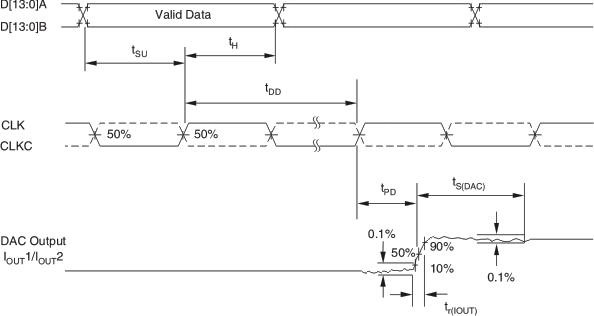 Figure 1. Timing Diagram
7.8 Electrical Characteristics(1)
over operating junction temperature range, AVDD = 3.3 V, DVDD = 3.3 V, IO(FS) = 20 mA (unless otherwise noted)| APPLIED VOLTAGES | RESULTING DIFFERENTIAL INPUT VOLTAGE | RESULTING COMMON-MODE INPUT VOLTAGE | LOGICAL BIT BINARY EQUIVALENT | COMMENT | |
|---|---|---|---|---|---|
| VA (V) | VB (V) | VA,B (mV) | VCOM (V) | ||
| 1.25 | 1.15 | 100 | 1.2 | 1 | Operation with minimum differential voltage (±100 mV) applied to the complementary inputs versus common-mode range |
| 1.15 | 1.25 | –100 | 1.2 | 0 | |
| 2.4 | 2.3 | 100 | 2.35 | 1 | |
| 2.3 | 2.4 | –100 | 2.35 | 0 | |
| 0.1 | 0 | 100 | 0.05 | 1 | |
| 0 | 0.1 | –100 | 0.05 | 0 | |
| 1.5 | 0.9 | 600 | 1.2 | 1 | Operation with maximum differential voltage (±600 mV) applied to the complementary inputs versus common-mode range |
| 0.9 | 1.5 | –600 | 1.2 | 0 | |
| 2.4 | 1.8 | 600 | 2.1 | 1 | |
| 1.8 | 2.4 | –600 | 2.1 | 0 | |
| 0.6 | 0 | 600 | 0.3 | 1 | |
| 0 | 0.6 | –600 | 0.3 | 0 | |
(1) Specifications subject to change.
 Figure 2. LVDS Timing Test Circuit and Input Test Levels
7.9 Typical Characteristics
