SLAS464C December 2006 – January 2018 DAC8560
PRODUCTION DATA.
- 1 Features
- 2 Applications
- 3 Description
- 4 Revision History
- 5 Pin Configuration and Functions
-
6 Specifications
- 6.1 Absolute Maximum Ratings
- 6.2 ESD Ratings
- 6.3 Recommended Operating Conditions
- 6.4 Thermal Information
- 6.5 Electrical Characteristics
- 6.6 Timing Requirements
- 6.7 Typical Characteristics: Internal Reference
- 6.8 Typical Characteristics: DAC at VDD = 5 V
- 6.9 Typical Characteristics: DAC at VDD = 3.6 V
- 6.10 Typical Characteristics: DAC at VDD = 2.7 V
-
7 Detailed Description
- 7.1 Overview
- 7.2 Functional Block Diagram
- 7.3 Feature Description
- 7.4 Device Functional Modes
- 7.5 Programming
- 7.6 Register Maps
- 8 Application and Implementation
- 9 Power Supply Recommendations
- 10Layout
- 11Device and Documentation Support
- 12Mechanical, Packaging, and Orderable Information
Package Options
Mechanical Data (Package|Pins)
- DGK|8
Thermal pad, mechanical data (Package|Pins)
Orderable Information
8.2.2.1.1 Passive Component Selection
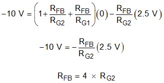
The amplifier in this circuit uses negative feedback to ensure that the voltages at the inverting and non-inverting terminals are equal. When the DAC output is at zero scale (0 V) the inverting terminal is a virtual ground so no current flows across RG1; this causes the circuit to function as an inverting amplifier with gain equal to RFB / RG2. When the DAC output is full-scale (VREF) the inverting terminal potential is equal to VREF so no current flows across RG2; this causes the circuit to function as a non-inverting amplifier with gain equal to (1 + RFB / RG1). A simple three-step process can be used to select the resistor values used to realize any bipolar output range using DAC8560. The internal VREF value is 2.5 V. The desired output range for this design is ±10 V. First, using the transfer function shown in Equation 6, consider the negative full-scale output case when VDAC is equal to 0 V, VREF is equal to 2.5 V, and VOUT is equal to –10 V. This case is used to calculate the ratio of RFB to RG2 and is shown explicitly in Equation 7.

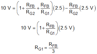
Second, consider the positive full-scale output case when VDAC is equal to 2.5 V, VREF is equal to 2.5 V, and VOUT is equal to 10 V. This case is used to calculate the ratio of RFB to RG1 and is shown explicitly in Equation 8.

Finally, seed the ideal value of RG2 to calculate the ideal values of RFB and RG2. The key considerations for seeding the value of RG2 should be the drive strength of the reference source as well as choosing small resistor values to minimize noise contributed by the resistor network. For this design RG2 of 8.25 kΩ was chosen, which limits the peak current drawn from the reference source to approximately 333 µA under nominal conditions, well within the 20-mA limit of the DAC8560. In this case the nearest, 0.1% tolerance, 0603 package values for each resistor are ideal.
Standard values for 0.1% resistors can be an obstacle for this design and it may take multiple iterations of seeding the values to find real components or they may not exist. Workarounds can include utilizing multiple resistors in series and/or parallel, using potentiometers for analog trim calibration, or providing extra gain in the output circuit and applying digital calibration. In systems where the output voltage must reach the design-goal end-points (±10 V) it may be desirable to apply additional gain to the circuit. This approach may contribute additional overall system error since the end-point errors vary from system to system. For this design, use the exact values calculated in the design process to keep error analysis easy to follow.
To deliver a near-universal cable drive solution, choose CLOAD to be relatively large compared to typical cable capacitance such that its capacitance dominates the reactive load seen by the output amplifier. To drive larger capacitive loads RISO, CCOMP, and CLOAD may need to be adjusted. An RISO of 70 Ω and CCOMP of 150 pF are used for this design.
Resistor matching for the op amp resistor network is critical for the success of this design; choose components with tight tolerances. For this design 0.1% resistor values are implemented but this constraint may be adjusted based on application specific design goals. Resistor matching contributes to both offset error and gain error in this design. The tolerance of stability components RISO and CCOMP is not critical and 1% components are acceptable.
Table 3. Values of Resistor Network
| RESISTOR | VALUE |
| RG1 | 11 kΩ |
| RG2 | 8.25 kΩ |
| RFB | 33 kΩ |