SBAS349F August 2005 – June 2016 DAC8812
PRODUCTION DATA.
- 1 Features
- 2 Applications
- 3 Description
- 4 Revision History
- 5 Device Comparison Table
- 6 Pin Configuration and Functions
- 7 Specifications
- 8 Detailed Description
- 9 Application and Implementation
- 10Power Supply Recommendations
- 11Layout
- 12Device and Documentation Support
- 13Mechanical, Packaging, and Orderable Information
Package Options
Mechanical Data (Package|Pins)
- PW|16
Thermal pad, mechanical data (Package|Pins)
Orderable Information
8 Detailed Description
8.1 Overview
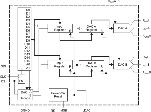
The DAC8812 contains two 16-bit, current-output, digital-to-analog converters (DACs). Each DAC has its own independent multiplying reference input. The DAC8812 uses a 3-wire, SPI-compatible serial data interface, with a configurable asynchronous RS pin for midscale (MSB = 1) or zero-scale (MSB = 0) preset. In addition, an LDAC strobe enables two channel simultaneous updates for hardware synchronized output voltage changes.
8.2 Functional Block Diagram
8.3 Feature Description
8.3.1 Digital-to-Analog Converters
The DAC8812 contains two current-steering R-2R ladder DACs. Figure 30 shows a typical equivalent DAC. Each DAC contains a matching feedback resistor for use with an external I-to-V converter amplifier. The RFBX pin is connected to the output of the external amplifier. The IOUTX pin is connected to the inverting input of the external amplifier. The AGNDX pin should be Kelvin-connected to the load point in the circuit requiring the full 16-bit accuracy.
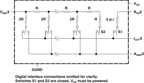 Figure 30. Typical Equivalent DAC Channel
The DAC is designed to operate with both negative or positive reference voltages. The VDD power pin is only used by the logic to drive the DAC switches on and off. Note that a matching switch is used in series with the internal 5 kΩ feedback resistor. If users are attempting to measure the value of RFB, power must be applied to VDD in order to achieve continuity. The DAC output voltage is determined by VREF and the digital data (D) according to Equation 1:
Note that the output polarity is opposite of the VREF polarity for dc reference voltages.
The DAC is also designed to accommodate ac reference input signals. The DAC8812 accommodates input reference voltages in the range of –15 V to 15 V. The reference voltage inputs exhibit a constant nominal input resistance of 5 kΩ, ±20%. On the other hand, DAC outputs IOUTA and B are code-dependent and produce various output resistances and capacitances.
The choice of external amplifier should take into account the variation in impedance generated by the DAC8812 on the amplifiers' inverting input node. The feedback resistance, in parallel with the DAC ladder resistance, dominates output voltage noise. For multiplying mode applications, an external feedback compensation capacitor, CFB (4 pF to 20 pF typical), may be needed to provide a critically damped output response for step changes in reference input voltages.
Figure 15 shows the gain vs frequency performance at various attenuation settings using a 3 pF external feedback capacitor connected across the IOUTX and RFBX pins. In order to maintain good analog performance, power-supply bypassing of 0.01 μF, in parallel with 1 μF, is recommended. Under these conditions, clean power supply with low ripple voltage capability should be used. Switching power supplies is usually not suitable for this application due to the higher ripple voltage and PSS frequency-dependent characteristics. It is best to derive the DAC8812 5-V supply from the system analog supply voltages (do not use the digital 5-V supply); see Figure 31.
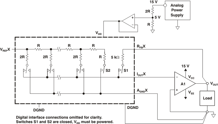 Figure 31. Recommended Kelvin-Sensed Hookup
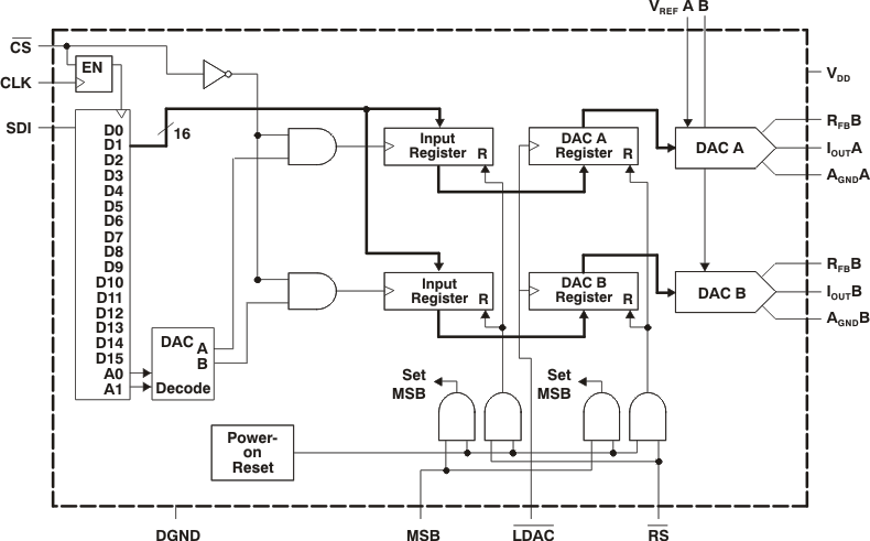 Figure 32. System-Level Digital Interfacing
8.3.2 Power-On Reset
When the VDD power supply is turned on, an internal reset strobe forces all the Input and DAC registers to the zero-code state or midscale, depending on the MSB pin voltage. The VDD power supply should have a smooth positive ramp without drooping, in order to have consistent results, especially in the region of VDD = 1.5 V to
2.3 V. The DAC register data stays at zero or midscale setting until a valid serial register data load takes place.
8.3.2.1 ESD Protection Circuits
All logic-input pins contain back-biased ESD protection zener diodes connected to ground (DGND) and VDD as shown in Figure 33.
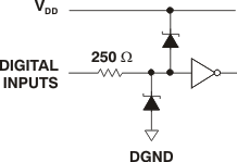 Figure 33. Equivalent ESD Protection Circuits
8.4 Device Functional Modes
8.4.1 Serial Data Interface
The DAC8812 uses a 3-wire (CS, SDI, CLK) SPI-compatible serial data interface. Serial data of the DAC8812 is clocked into the serial input register in an 18-bit data-word format. MSB bits are loaded first. Table 1 defines the 18 data-word bits for the DAC8812.
Data is placed on the SDI pin, and clocked into the register on the positive clock edge of CLK subject to the data setup and data hold time requirements specified in the Interface Timing specifications of the Electrical Characteristics. Data can only be clocked in while the CS chip select pin is active low. For the DAC8812, only the last 18 bits clocked into the serial register are interrogated when the CS pin returns to the logic high state.
Because most microcontrollers output serial data in 8-bit bytes, three right-justified data bytes can be written to the DAC8812. Keeping the CS line low between the first, second, and third byte transfers will result in a successful serial register update.
When the data is properly aligned in the shift register, the positive edge of the CS initiates the transfer of new data to the target DAC register, determined by the decoding of address bits A1 and A0. For the DAC8812, Table 1, Table 2, Table 3, and Figure 1 define the characteristics of the software serial interface.
Table 1. Serial Input Register Data Format, Data Loaded MSB First(1)
| Bit | B17 (MSB) | B16 | B15 | B14 | B13 | B12 | B11 | B10 | B9 | B8 | B7 | B6 | B5 | B4 | B3 | B2 | B1 | B0 (LSB) |
| Data | A1 | A0 | D15 | D14 | D13 | D12 | D11 | D10 | D9 | D8 | D7 | D6 | D5 | D4 | D3 | D2 | D1 | D0 |
Table 2. Control Logic Truth Table(1)
| CS | CLK | LDAC | RS | MSB | SERIAL SHIFT REGISTER | INPUT REGISTER | DAC REGISTER |
|---|---|---|---|---|---|---|---|
| H | X | H | H | X | No effect | Latched | Latched |
| L | L | H | H | X | No effect | Latched | Latched |
| L | ↑+ | H | H | X | Shift register data advanced one bit | Latched | Latched |
| L | H | H | H | X | No effect | Latched | Latched |
| ↑+ | L | H | H | X | No effect | Selected DAC updated with current SR contents | Latched |
| H | X | L | H | X | No effect | Latched | Transparent |
| H | X | H | H | X | No effect | Latched | Latched |
| H | X | ↑+ | H | X | No effect | Latched | Latched |
| H | X | H | L | 0 | No effect | Latched data = 0000h | Latched data = 0000h |
| H | X | H | L | H | No effect | Latched data = 8000h | Latched data = 8000h |
Table 3. Address Decode
| A1 | A0 | DAC DECODE |
|---|---|---|
| 0 | 0 | None |
| 0 | 1 | DAC A |
| 1 | 0 | DAC B |
| 1 | 1 | DAC A and DAC B |
Figure 34 shows the equivalent logic interface for the key digital control pins for the DAC8812.
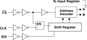 Figure 34. DAC8812 Equivalent Logic Interface
Two additional pins, RS and MSB, provide hardware control over the preset function and DAC register loading. If these functions are not needed, the RS pin can be tied to logic high. The asynchronous input RS pin forces all input and DAC registers to either the zero-code state (MSB = 0), or the midscale state (MSB = 1).
