SBAS438C May 2008 – November 2019 DAC9881
PRODUCTION DATA.
- 1 Features
- 2 Applications
- 3 Description
- 4 Revision History
- 5 Pin Configuration and Functions
-
6 Specifications
- 6.1 Absolute Maximum Ratings
- 6.2 ESD Ratings
- 6.3 Recommended Operating Conditions
- 6.4 Thermal Information
- 6.5 Electrical Characteristics: AVDD = 5 V
- 6.6 Electrical Characteristics: AVDD = 2.7 V
- 6.7 Timing Requirements—Standalone Operation Without SDO
- 6.8 Timing Requirements—Standalone Operation With SDO and Daisy-Chain Mode
- 6.9 Typical Characteristics: AVDD = 5 V
- 6.10 Typical Characteristics: AVDD = 2.7 V
-
7 Detailed Description
- 7.1 Overview
- 7.2 Functional Block Diagram
- 7.3 Feature Description
- 7.4 Device Functional Modes
- 8 Application and Implementation
- 9 Power Supply Recommendations
- 10Layout
- 11Device and Documentation Support
- 12Mechanical, Packaging, and Orderable Information
Package Options
Mechanical Data (Package|Pins)
- RGE|24
Thermal pad, mechanical data (Package|Pins)
- RGE|24
Orderable Information
8.3 System Example
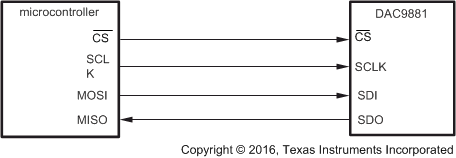
Figure 75 displays a typical serial interface that may be used when connecting the DAC9881's SPI serial interface to a (master) microcontroller. The setup for the interface is as follows: The microcontroller's output SPI CLK drives the SCLK pin of the DAC9881, while the DAC9881 SDI pin is driven by the MOSI pin of the microcontroller. The CS pin of the DAC9881 can be asserted from a general program input/output pin of the microcontroller. When data are to be transmitted to the DAC9881, the CS pint is taken low. The data from the microcontroller is then transmitted to the DAC9881, totaling 24 bits latched into the DAC9881 device through the negative edge of SCLK. CS is then brought high after the completed write. The DAC9881 requires its data with the MSB as the first bit received.
 Figure 75. Simplified Sample-and-Hold Circuit