DLPS147B January   2019  – May 2022 DLP4500NIR

PRODUCTION DATA  

  1. Features
  2. Applications
  3. Description
  4. Revision History
  5. Chipset Component Usage Specification
  6. Pin Configuration and Functions
  7. Specifications
    1. 7.1  Absolute Maximum Ratings
    2. 7.2  Storage Conditions
    3. 7.3  ESD Ratings
    4. 7.4  Recommended Operating Conditions
    5. 7.5  Thermal Information
    6. 7.6  Electrical Characteristics
    7. 7.7  Timing Requirements
    8. 7.8  System Mounting Interface Loads
    9. 7.9  Micromirror Array Physical Characteristics
    10. 7.10 Micromirror Array Optical Characteristics
    11. 7.11 Typical Characteristics
  8. Detailed Description
    1. 8.1 Overview
    2. 8.2 Functional Block Diagram
    3. 8.3 Feature Description
    4. 8.4 Device Functional Modes
      1. 8.4.1 Operating Modes
    5. 8.5 Micromirror Array Temperature Calculation
      1. 8.5.1 Package Thermal Resistance
      2. 8.5.2 Case Temperature
        1. 8.5.2.1 Temperature Calculation
    6. 8.6 Micromirror Landed-on/Landed-Off Duty Cycle
      1. 8.6.1 Definition of Micromirror Landed-On/Landed-Off Duty Cycle
      2. 8.6.2 Landed Duty Cycle and Useful Life of the DMD
      3. 8.6.3 Landed Duty Cycle and Operational DMD Temperature
      4. 8.6.4 Estimating the Long-Term Average Landed Duty Cycle of a Product or Application
  9. Applications and Implementation
    1. 9.1 Application Information
    2. 9.2 Typical Application
      1. 9.2.1 Design Requirements
      2. 9.2.2 Detailed Design Procedure
        1. 9.2.2.1 DLPC350 System Interfaces
          1. 9.2.2.1.1 Control Interface
          2. 9.2.2.1.2 Input Data Interface
        2. 9.2.2.2 DLPC350 System Output Interfaces
          1. 9.2.2.2.1 Illumination Interface
          2. 9.2.2.2.2 Trigger Interface (Sync Outputs)
        3. 9.2.2.3 DLPC350 System Support Interfaces
          1. 9.2.2.3.1 Reference Clock
          2. 9.2.2.3.2 PLL
          3. 9.2.2.3.3 Program Memory Flash Interface
        4. 9.2.2.4 DMD Interfaces
          1. 9.2.2.4.1 DLPC350 to DMD Digital Data
          2. 9.2.2.4.2 DLPC350 to DMD Control Interface
          3. 9.2.2.4.3 DLPC350 to DMD Micromirror Reset Control Interface
  10. 10Power Supply Recommendations
    1. 10.1 Power Supply Sequencing Requirements
    2. 10.2 DMD Power Supply Power-Up Procedure
    3. 10.3 DMD Power Supply Power-Down Procedure
  11. 11Layout
    1. 11.1 Layout Guidelines
      1. 11.1.1 DMD Interface Design Considerations
      2. 11.1.2 DMD Termination Requirements
      3. 11.1.3 Decoupling Capacitors
      4. 11.1.4 Power Plane Recommendations
      5. 11.1.5 Signal Layer Recommendations
      6. 11.1.6 General Handling Guidelines for CMOS-Type Pins
      7. 11.1.7 PCB Manufacturing
        1. 11.1.7.1 General Guidelines
        2. 11.1.7.2 Trace Widths and Minimum Spacings
        3. 11.1.7.3 Routing Constraints
        4. 11.1.7.4 Fiducials
        5. 11.1.7.5 Flex Considerations
        6. 11.1.7.6 DLPC350 Thermal Considerations
    2. 11.2 Layout Example
      1. 11.2.1 Printed Circuit Board Layer Stackup Geometry
      2. 11.2.2 Recommended DLPC350 MOSC Crystal Oscillator Configuration
      3. 11.2.3 Recommended DLPC350 PLL Layout Configuration
  12. 12Device and Documentation Support
    1. 12.1 Device Support
      1. 12.1.1 Third-Party Products Disclaimer
      2. 12.1.2 Device Nomenclature
      3. 12.1.3 Device Markings
    2. 12.2 Documentation Support
      1. 12.2.1 Related Documentation
    3. 12.3 Receiving Notification of Documentation Updates
    4. 12.4 Support Resources
    5. 12.5 Trademarks
    6. 12.6 Electrostatic Discharge Caution
    7. 12.7 Glossary
  13. 13Mechanical, Packaging, and Orderable Information

Package Options

Mechanical Data (Package|Pins)
Thermal pad, mechanical data (Package|Pins)
Orderable Information

Printed Circuit Board Layer Stackup Geometry

The DLPC350 PCB is targeted at six layers with layer stack up shown in Figure 11-2. The PCB layer stack may vary depending on system design. However, careful attention is required to meet design considerations. Layers one and six should consist of the components layers. Low-speed routing and power splits are allowed on these layers. Layer two should consist of a solid ground plane. Layer five should be a split voltage plane. Layers three and four should be used as the primary routing layers. Routing on external layers should be less than 0.25 inches for priority one and two signals. Refer to Table 11-7 for signal priority groups.

Board material should be FR-370HR or similar. PCB should be designed for lead-free assembly with the stackup geometry shown in Figure 11-2.
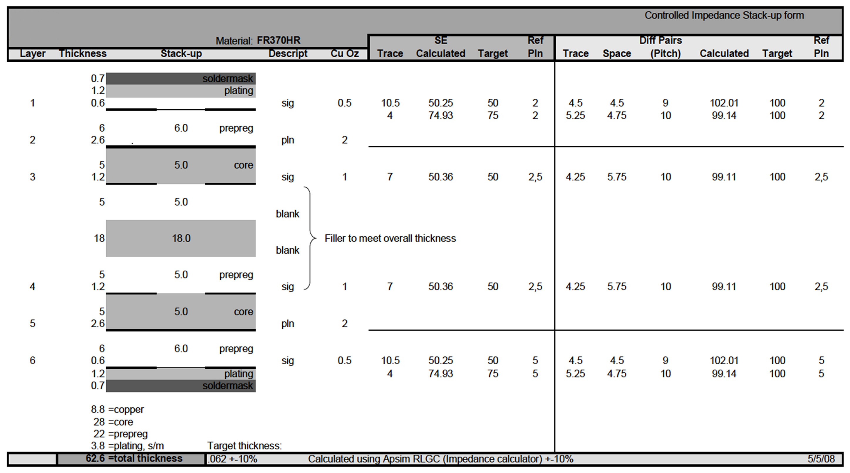
GUID-B00442FD-93C3-431E-96F6-FAAB80E3F23A-low.pngFigure 11-2 Layer Stackup
Table 11-10 PCB Layer Stackup Geometry
PARAMETERDESCRIPTIONRECOMMENDATION
Reference plane 1Ground plane for proper return
Reference plane 21.9-V DMD I/O power plane or ground
ErDielectric FR44.3 at 1 GHz (nominal)
H1Signal trace distance to reference plane 15 mil (0.127 mm)
H2Signal trace distance to reference plane 230.4 mil