DLPS097A August 2017 – February 2023 DLP650NE
PRODUCTION DATA
- 1 Features
- 2 Applications
- 3 Description
- 4 Revision History
- 5 Pin Configuration and Functions
-
6 Specifications
- 6.1 Absolute Maximum Ratings
- 6.2 Storage Conditions
- 6.3 ESD Ratings
- 6.4 Recommended Operating Conditions
- 6.5 Thermal Information
- 6.6 Electrical Characteristics
- 6.7 Timing Requirements
- 6.8 Window Characteristics
- 6.9 System Mounting Interface Loads
- 6.10 Micromirror Array Physical Characteristics
- 6.11 Micromirror Array Optical Characteristics
- 6.12 Chipset Component Usage Specification
-
7 Detailed Description
- 7.1 Overview
- 7.2 Functional Block Diagram
- 7.3 Feature Description
- 7.4 Device Functional Modes
- 7.5 Optical Interface and System Image Quality Considerations
- 7.6 Micromirror Array Temperature Calculation
- 7.7 Micromirror Landed-On or Landed-Off Duty Cycle
- 8 Power Supply Requirements
- 9 Device Documentation Support
- 10Mechanical, Packaging, and Orderable Information
Package Options
Refer to the PDF data sheet for device specific package drawings
Mechanical Data (Package|Pins)
- FYE|350
Thermal pad, mechanical data (Package|Pins)
Orderable Information
6.11 Micromirror Array Optical Characteristics
See GUID-90EC14FF-C808-445F-A737-95EF6292FA0E.html#GUID-90EC14FF-C808-445F-A737-95EF6292FA0E
for important information.
| PARAMETER | MIN | NOM | MAX | UNIT | ||
|---|---|---|---|---|---|---|
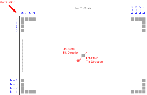
| Mirror tilt angle, variation device to device#DLPS0364269#DLPS0362219#T4931159-41#DLPS0362972 | 11 | 12 | 13 | ° | ||
| Number of out-of-specification micromirrors#T4931159-34 | Adjacent micromirrors | 0 | micromirrors | |||
| Non-adjacent micromirrors | 10 | |||||
(1) Measured relative to the plane formed by the overall micromirror
array
(2) Variation can occur between any two individual micromirrors located on the same device or located on different devices.
(3) Additional
variation exists between the
micromirror
array and the
package
datums. See
the
package drawing.
(4) See #DLPS0367592.
(5) An
"out-of-specification
micromirror"
is defined as a micromirror that is unable to transition between the two landed
states.

Refer to
Micromirror Array Physical Characteristics
for
M, N, and P specifications.
Figure 6-12 Micromirror Landed Orientation and Tilt