DLPS097A August 2017 – February 2023 DLP650NE
PRODUCTION DATA
- 1 Features
- 2 Applications
- 3 Description
- 4 Revision History
- 5 Pin Configuration and Functions
-
6 Specifications
- 6.1 Absolute Maximum Ratings
- 6.2 Storage Conditions
- 6.3 ESD Ratings
- 6.4 Recommended Operating Conditions
- 6.5 Thermal Information
- 6.6 Electrical Characteristics
- 6.7 Timing Requirements
- 6.8 Window Characteristics
- 6.9 System Mounting Interface Loads
- 6.10 Micromirror Array Physical Characteristics
- 6.11 Micromirror Array Optical Characteristics
- 6.12 Chipset Component Usage Specification
-
7 Detailed Description
- 7.1 Overview
- 7.2 Functional Block Diagram
- 7.3 Feature Description
- 7.4 Device Functional Modes
- 7.5 Optical Interface and System Image Quality Considerations
- 7.6 Micromirror Array Temperature Calculation
- 7.7 Micromirror Landed-On or Landed-Off Duty Cycle
- 8 Power Supply Requirements
- 9 Device Documentation Support
- 10Mechanical, Packaging, and Orderable Information
Package Options
Refer to the PDF data sheet for device specific package drawings
Mechanical Data (Package|Pins)
- FYE|350
Thermal pad, mechanical data (Package|Pins)
Orderable Information
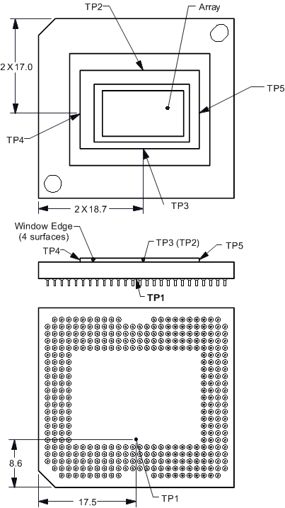
7.6 Micromirror Array Temperature Calculation
 Figure 7-1 DMD Thermal Test Points
Micromirror array temperature cannot be measured directly, therefore it must be computed analytically from measurement points on the outside of the package, the package thermal resistance, the electrical power, and the illumination heat load. The relationship between array temperature and the reference ceramic temperature (thermal test TP1 in #DLPS0363628) is provided by the following equations:
where
- TARRAY = Computed array temperature (°C)
- TCERAMIC = measured ceramic temperature (°C), TP1 location in #DLPS0363628
- RARRAY–TO–CERAMIC = thermal resistance of package (specified in Thermal Information) from array to ceramic TP1 (°C/W)
- QARRAY = total DMD Power on array (W). (electrical + absorbed)
- QELECTRICAL = Nominal DMD electrical power dissipation (W)
- CL2W = Conversion constant for screen lumens to absorbed optical power on the DMD (W/lm) specified below
- SL = Measured ANSI screen lumens (lm)
The electrical power dissipation of the DMD is variable and depends on the voltages, data rates and operating frequencies. The nominal electrical power dissipation to use when calculating array temperature is 2.9 W. The absorbed optical power from the illumination source is variable and depends on the operating state of the micromirrors and the intensity of the light source. The equations shown above are valid for a 1-chip DMD system with total projection efficiency through the projection lens from DMD to the screen of 87%.
The conversion constant CL2W is based on the DMD micromirror array characteristics. It assumes a spectral efficiency of 300 lm/W for the projected light and illumination distribution of 83.7% on the DMD active array, and 16.3% on the DMD array border and window aperture. The conversion constant is calculated to be 0.00293 W/lm.
Sample calculations: