DLPS153 October 2023 DLP651LE
PRODUCTION DATA
- 1
- 1 Features
- 2 Applications
- 3 Description
- 4 Revision History
- 5 Pin Configuration and Functions
-
6 Specifications
- 6.1 Absolute Maximum Ratings
- 6.2 Storage Conditions
- 6.3 ESD Ratings
- 6.4 Recommended Operating Conditions
- 6.5 Thermal Information
- 6.6 Electrical Characteristics
- 6.7 Timing Requirements
- 6.8 System Mounting Interface Loads
- 6.9 Micromirror Array Physical Characteristics
- 6.10 Micromirror Array Optical Characteristics
- 6.11 Window Characteristics
- 6.12 Chipset Component Usage Specification
-
7 Detailed Description
- 7.1 Overview
- 7.2 Functional Block Diagram
- 7.3 Feature Description
- 7.4 Optical Interface and System Image Quality Considerations
- 7.5 Micromirror Array Temperature Calculation
- 7.6 Micromirror Power Density Calculation
- 7.7 Window Aperture Illumination Overfill Calculation
- 7.8 Micromirror Landed-On/Landed-Off Duty Cycle
- 8 Application and Implementation
- 9 Layout
- 10Power Supply Recommendations
- 11Device and Documentation Support
- 12Mechanical, Packaging, and Orderable Information
Package Options
Mechanical Data (Package|Pins)
- FYM|149
Thermal pad, mechanical data (Package|Pins)
Orderable Information
7.5 Micromirror Array Temperature Calculation
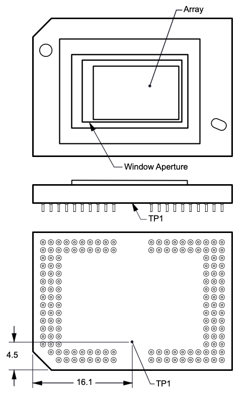
 Figure 7-1 DMD Thermal Test
Points
Figure 7-1 DMD Thermal Test
PointsMicromirror array temperature cannot be measured directly, therefore it must be computed analytically from measurement points on the outside of the package, the package thermal resistance, the electrical power, and the illumination heat load. The relationship between array temperature and the reference ceramic temperature (thermal test TP1 in Figure 7-1) is provided by the following equations:
Equation 1. TARRAY = TCERAMIC + (QARRAY ×
RARRAY-TO-CERAMIC)
Equation 2. QARRAY = QELECTRICAL +
QILLUMINATION
where
- TARRAY = Computed array temperature (°C)
- TCERAMIC = Measured ceramic temperature (°C) (TP1 location)
- RARRAY-TO-CERAMIC = Thermal resistance of package specified in Section 6.5 from array to ceramic TP1 (°C/Watt)
- QARRAY = Total DMD power on the array (W) (electrical + absorbed)
- QELECTRICAL = Nominal Electrical Power (W)
- QINCIDENT = Incident illumination optical power (W)
- QILLUMINATION = (DMD average thermal absorptivity × QINCIDENT) (W)
- DMD average thermal absorptivity = 0.42
The sample calculation for a typical projection application is as follows:
Equation 3. QINCIDENT = 45 W
(measured)
TCERAMIC = 55.0°C
QELECTRICAL = 1.5 W
QARRAY = 1.5 W + (0.42 × 45 W) =
20.4 W
TARRAY = 55.0°C + (20.4 W × 0.50°C/W) = 65.2 °C