DLPS029F April   2013  – May 2019 DLPC350

PRODUCTION DATA.  

  1. Features
  2. Applications
  3. Description
    1.     Simplified Application
  4. Revision History
  5. Pin Configuration and Functions
    1.     Pin Functions
    2. Table 1. Power and Ground Pin Descriptions
  6. Specifications
    1. 6.1  Absolute Maximum Ratings
    2. 6.2  ESD Ratings
    3. 6.3  Recommended Operating Conditions
    4. 6.4  Thermal Information
    5. 6.5  I/O Electrical Characteristics
    6. 6.6  I2C0 and I2C1 Interface Timing Requirements
    7. 6.7  Port 1 Input Pixel Interface Timing Requirements
    8. 6.8  Port 2 Input Pixel Interface (FPD-Link Compatible LVDS Input) Timing Requirements
    9. 6.9  System Oscillator Timing Requirements
    10. 6.10 Reset Timing Requirements
    11. 6.11 Video Timing Input Blanking Specification
      1. 6.11.1 Source Input Blanking
    12. 6.12 Programmable Output Clocks Switching Characteristics
    13. 6.13 DMD Interface Switching Characteristics
    14. 6.14 JTAG Interface: I/O Boundary Scan Application Switching Characteristics
  7. Parameter Measurement Information
    1. 7.1 Power Consumption
  8. Detailed Description
    1. 8.1 Overview
    2. 8.2 Functional Block Diagram
    3. 8.3 Feature Description
      1. 8.3.1 Board Level Test Support
    4. 8.4 Device Functional Modes
      1. 8.4.1 Structured Light Applications
      2. 8.4.2 (LVDS) Receiver Supported Pixel Mapping Modes
  9. Application and Implementation
    1. 9.1 Application Information
    2. 9.2 Typical Applications
      1. 9.2.1 Typical Chipset Application
        1. 9.2.1.1 Design Requirements
        2. 9.2.1.2 Detailed Design Procedure
          1. 9.2.1.2.1 DLPC350 System Interfaces
            1. 9.2.1.2.1.1 Control Interface
            2. 9.2.1.2.1.2 Input Data Interface
          2. 9.2.1.2.2 DLPC350 System Output Interfaces
            1. 9.2.1.2.2.1 Illumination Interface
            2. 9.2.1.2.2.2 Trigger Interface (Sync Outputs)
          3. 9.2.1.2.3 DLPC350 System Support Interfaces
            1. 9.2.1.2.3.1 Reference Clock
            2. 9.2.1.2.3.2 PLL
            3. 9.2.1.2.3.3 Program Memory Flash Interface
          4. 9.2.1.2.4 DMD Interfaces
            1. 9.2.1.2.4.1 DLPC350 to DMD Digital Data
            2. 9.2.1.2.4.2 DLPC350 to DMD Control Interface
            3. 9.2.1.2.4.3 DLPC350 to DMD Micromirror Reset Control Interface
  10. 10Power Supply Recommendations
    1. 10.1 System Power and Reset
      1. 10.1.1 Default Conditions
        1. 10.1.1.1 1.2-V System Power
        2. 10.1.1.2 1.8-V System Power
        3. 10.1.1.3 1.9-V System Power
        4. 10.1.1.4 3.3-V System Power
        5. 10.1.1.5 FPD-Link Input LVDS System Power
      2. 10.1.2 System Power-up and Power-down Sequence
      3. 10.1.3 Power-On Sense (POSENSE) Support
      4. 10.1.4 Power-Good (PWRGOOD) Support
      5. 10.1.5 5-V Tolerant Support
      6. 10.1.6 Power Reset Operation
      7. 10.1.7 System Reset Operation
  11. 11Layout
    1. 11.1 Layout Guidelines
      1. 11.1.1 DMD Interface Design Considerations
      2. 11.1.2 DMD Termination Requirements
      3. 11.1.3 Decoupling Capacitors
      4. 11.1.4 Power Plane Recommendations
      5. 11.1.5 Signal Layer Recommendations
      6. 11.1.6 General Handling Guidelines for CMOS-Type Pins
      7. 11.1.7 PCB Manufacturing
        1. 11.1.7.1 General Guidelines
        2. 11.1.7.2 Trace Widths and Minimum Spacings
        3. 11.1.7.3 Routing Constraints
        4. 11.1.7.4 Fiducials
        5. 11.1.7.5 Flex Considerations
        6. 11.1.7.6 DLPC350 Thermal Considerations
    2. 11.2 Layout Example
      1. 11.2.1 Printed Circuit Board Layer Stackup Geometry
      2. 11.2.2 Recommended DLPC350 MOSC Crystal Oscillator Configuration
      3. 11.2.3 Recommended DLPC350 PLL Layout Configuration
  12. 12Device and Documentation Support
    1. 12.1 Device Support
      1. 12.1.1 Video Timing Parameter Definitions
      2. 12.1.2 Device Nomenclature
      3. 12.1.3 Device Marking
    2. 12.2 Documentation Support
      1. 12.2.1 Related Documentation
    3. 12.3 Trademarks
    4. 12.4 Glossary
  13. 13Mechanical, Packaging, and Orderable Information
    1. 13.1 Package Option Addendum
      1. 13.1.1 Packaging Information

Package Options

Mechanical Data (Package|Pins)
Thermal pad, mechanical data (Package|Pins)

Reset Timing Requirements

PARAMETER MIN MAX UNIT
tw1(L) Pulse duration, inactive low, PWRGOOD 50% reference points 4 µs
tt1 Transition time, PWRGOOD 20% to 80% reference points 625 µs
tw2(L) Pulse duration, inactive low, POSENSE 50% reference points 500 µs
tt2 Transition time, POSENSE 20% to 80% reference points 1 µs
tPH Power hold time, POSENSE remains active after PWRGOOD is de-asserted 20% to 80% reference points 500 µs
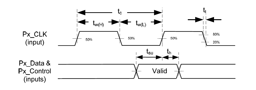
DLPC350 Port1_Timing_DLPS029.pngFigure 1. Port 1 Input Pixel Timing
DLPC350 LVDS_Start_Up_DLPS029.pngFigure 2. LVDS Timing Diagram
DLPC350 LVDS_Data_Skew_DLPS029.pngFigure 3. (LVDS) Link Start-up Timing
DLPC350 Port2_Timing_DLPS029.pngFigure 4. (LVDS) Clock: Data Skew Definition
DLPC350 System_Oscillators_Timing_DLPS029.pngFigure 5. System Oscillators Timing