DLPS167 March 2024 DLPC964
PRODUCTION DATA
- 1
- 1 Features
- 2 Applications
- 3 Description
- 4 Pin Configuration and Functions
- 5 Specifications
-
6 Detailed Description
- 6.1 Overview
- 6.2 Functional Block Diagram
- 6.3 Feature Description
- 6.4
Device Functional
Modes
- 6.4.1 DLPC964 Aurora 64B/66B Input Data and Command Write Cycle
- 6.4.2 DMD Row Operation
- 6.4.3 Block Load Address Select
- 6.4.4 Block Mode Select
- 6.4.5 Mirror Clocking Pulse (MCP)
- 6.5
Register Map
- 6.5.1
Register Table Overview
- 6.5.1.1 FPGA_INTERRUPT_STATUS Register
- 6.5.1.2 FPGA_INTERRUPT_ENABLE_CONTROL Register
- 6.5.1.3 FPGA_MAIN_STATUS Register
- 6.5.1.4 FPGA_VERSION Register
- 6.5.1.5 FPGA_MAIN_CTRL Register
- 6.5.1.6 SELF_TEST_REG Register
- 6.5.1.7 DMDIF_ERROR_STATUS_CLR Register
- 6.5.1.8 DMDIF_ERROR_STATUS Register
- 6.5.1.9 PRBS7_MACRO0_TEST_RESULT Register
- 6.5.1.10 PRBS7_MACRO1_TEST_RESULT Register
- 6.5.1.11 PRBS7_MACRO2_TEST_RESULT Register
- 6.5.1.12 PRBS7_MACRO3_TEST_RESULT Register
- 6.5.1.13 PRBS7_TEST_CONTROL Register
- 6.5.1.14 PRBS7_TEST_RUNSTATUS Register
- 6.5.1.15 LS_BUS_TEST_RESULT Register
- 6.5.1.16 DMD_TYPE Register
- 6.5.1.17 HSS_RESET Register
- 6.5.1.18 HSS_CHANNEL_STATUS Register
- 6.5.1.19 HSS_LANE_STATUS Register
- 6.5.1.20 HSS_CH0_SOFTERROR_COUNT Register
- 6.5.1.21 HSS_CH1_SOFTERROR_COUNT Register
- 6.5.1.22 HSS_CH2_SOFTERROR_COUNT Register
- 6.5.1.23 HSS_CH3_SOFTERROR_COUNT Register
- 6.5.1.24 HSS_SOFTERROR_COUNT_RESET Register
- 6.5.1.25 HSSI_Channel_0_DMD_Data_GT_Cell_Control Register
- 6.5.1.26 HSSI_Channel_0_DMD_Clock_GT_Cell_Control Register
- 6.5.1.27 HSSI_Channel_1_DMD_Data_GT_Cell_Control Register
- 6.5.1.28 HSSI_Channel_1_DMD_Clock_GT_Cell_Control Register
- 6.5.1.29 HSSI_Channel_2_DMD_Data_GT_Cell_Control Register
- 6.5.1.30 HSSI_Channel_2_DMD_Clock_GT_Cell_Control Register
- 6.5.1.31 HSSI_Channel_3_DMD_Data_GT_Cell_Control Register
- 6.5.1.32 HSSI_Channel_3_DMD_Clock_GT_Cell_Control Register
- 6.5.1.33 HSSI_DMD_Vcm_Value Register
- 6.5.1.34 TEST_DMD_ID Register
- 6.5.1.35 TEST_DMD_FUSE1 Register
- 6.5.1.36 TEST_DMD_FUSE2 Register
- 6.5.1.37 TEST_DMD_FUSE3 Register
- 6.5.1.38 TEST_DMD_FUSE4 Register
- 6.5.1
Register Table Overview
-
7 Application and Implementation
- 7.1 Application Information
- 7.2 Typical Application
- 7.3 Interfacing to DLPC964 Controller High Speed Serial (HSS) Aurora 64B/66B Inputs
- 7.4 Power Supply Recommendations
- 7.5 Layout
- 7.6 Layout Example
- 8 Device and Documentation Support
- 9 Revision History
- 10Mechanical, Packaging, and Orderable Information
Package Options
Refer to the PDF data sheet for device specific package drawings
Mechanical Data (Package|Pins)
- ZUM|1156
Thermal pad, mechanical data (Package|Pins)
Orderable Information
7.3.1.2 Block Complete with DMDLOAD_REQ
Refer to Figure 7-3, DMDLOAD_REQ is an output signal from the APPS FPGA to the DLPC964 Controller.
Once the Aurora Block Data transfer is complete, the APPS FPGA user logics must assert DMDLOAD_REQ to signal the end of a DMD block to the DLPC964 Controller and trigger the DLPC964 Controller to carry out the operation encoded in the Block Control Word.
Guidelines for asserting the DMDLOAD_REQ signal and sending the Block Control Word:
- APPS FPGA user logics must wait for the block data transfer to complete on all four Aurora data channels before asserting DMDLOAD_REQ. Asserting DMDLOAD_REQ before completion of the Aurora block data transfer can result in data not being properly loaded to the DMD. The APPS FPGA must take into account that the four Aurora data channel interfaces may not be fully synchronous to one another, thus data completion may not happen at the exact same clock cycle. Therefore, the APPS FPGA must monitor and ensure the Aurora block data transfer is completed on all four channels before asserting DMDLOAD_REQ.
- DMDLOAD_REQ may be asserted immediately after completing an Aurora block transfer as long as the 300ns DMDLOAD_REQ setup time is met (refer to Section 7.3.1.3 for more details).
- Apps user logics must assert DMDLOAD_REQ for the current block before initiating the transmission of the next new DMD block data. In other words, every block must start with a Block Control Word packet and end with DMDLOAD_REQ assertion.
- DMDLOAD_REQ is still required for operations that do not involve block data transfer (such as block-clear or block-set operation), and must still meet the required 300ns setup time (refer to Section 7.3.1.3 for more details).
- Refer to Figure 7-5. In most cases, after the APPS FPGA user logic has completed the transfer of the current data block, it may find that the DLPC964 Controller is still loading the previous block to the DMD (i.e. BLKLOADZ is low). If this occurs, the APPS FPGA can still assert DMDLOAD_REQ while BLKLOADZ is low. The DLPC964 Controller will detect and store the DMDLOAD_REQ request and perform the data load as soon as the transfer of the previous data block is complete.
- The DLPC964 Controller has two data-block buffers - one for receiving the incoming Aurora data block from the APPS FPGA, and the other for holding the previous data block for streaming out to the DMD. Care must be taken by the APPS FPGA to avoid overrunning these two buffers. Refer to Figure 7-5. After completing the current Aurora data transfer of block data and asserting the DMDLOAD_REQ signal, the APPS FPGA must wait for the de-assertion of BLKLOADZ by the DLPC964 Controller (i.e. BLKLOADZ transition from low to high) before starting the next block data transfer. De-assertion of BLKLOADZ indicates that the DLPC964 Controller has completed the DMD data loading operation for previous block, and a data buffer is freed up for accepting a new data block from the Aurora interface. The buffer will be overrun and data will be incorrectly loaded to the DMD if the APPS FPGA does not synchronize the Aurora block data transfer with BLKLOADZ signal de-assertion.
- It is not necessary for the APPS FPGA to immediately assert DMDLOAD_REQ after sending a DMD data block. The APPS FPGA may send the DLPC964 Controller a DMD data block and then delay the assertion of DMDLOAD_REQ until the system is ready for the DMD be loaded. Figure 7-6 describes this operation.
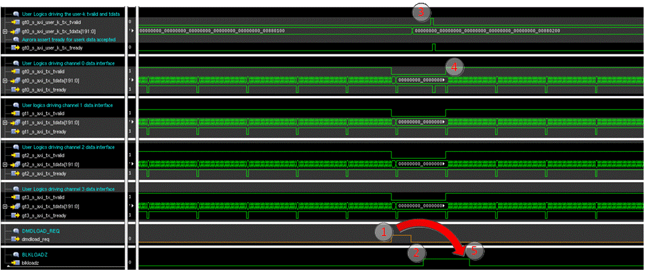
 Figure 7-5 End of Block DMDLOAD_REQ Assertion Followed by New Block Control Word Waveform.
 - APPS FPGA user logic asserts DMDLOAD_REQ immediately after the completion of current block data transmission on all four Aurora data interfaces.
- DLPC964 Controller de-asserts BLKLOADZ, indicating completion of the data loading operation for the previous DMD block.
- APPS FPGA user logics detects the de-assertion of BLKLOADZ and sends a new Block Control Word on Aurora Channel 0 User-K Port for the next block data.
- APPS FPGA user logics sending data for next block.
- BLKLOADZ is asserted low by the DLPC964 Controller, indicating the data loading operation for current block triggered by DMDLOAD_REQ occurred at 1.
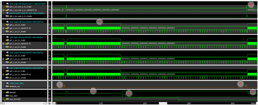
 Figure 7-6 DMDLOAD_REQ Delayed Assertion Waveform.
 - APPS FPGA finishes sending the last block data (block 15) of the current pattern and asserts DMDLOAD_REQ to instruct the DLPC964 Controller to carry out the data load operation.
- DLPC964 Controller loads data to block 15, triggered by DMDLOAD_REQ from 1.
- APPS FPGA sends the first block (block 0) of data for the next pattern over the Aurora data interfaces while the DLPC964 Controller is loading block 15 of the current pattern.
- DLPC964 de-asserts BLKLOADZ after completing the data load for block 15 of the current pattern. APPS FPGA detects the BLKLOADZ de-assertion (because the last block data of the current pattern has been loaded on to DMD) and issues an MCP_START signal for global block MCP operation. Notice that the DLPC964 Controller asserted the MCP0_ACTIVE signal to communicate that the MCP mirror operation in process.
- APPS FPGA delays the assertion of DMDLOAD_REQ for block 0 of next pattern due to the requirement of meeting the mirror settling time.
- APPS FPGA sends the Block Control Word for block 1 of the next pattern after the assertion of DMDLOAD_REQ for block 0.
- DLPC964 Controller asserts BLKLOADZ to indicate that the DMD data loading operation was triggered by DMDLOAD_REQ from 5.