SNLS341C March 2011 – March 2015 DP83848Q-Q1
PRODUCTION DATA.
- 1 Device Overview
- 2 Revision History
- 3 Pin Configuration and Functions
- 4 Specifications
-
5 Detailed Description
- 5.1 Overview
- 5.2 Functional Block Diagram
- 5.3 Feature Description
- 5.4 Device Functional Modes
- 5.5
Programming
- 5.5.1
Architecture
- 5.5.1.1 100BASE-TX Transmitter
- 5.5.1.2
100BASE-TX Receiver
- 5.5.1.2.1 Analog Front End
- 5.5.1.2.2 Digital Signal Processor
- 5.5.1.2.3 Signal Detect
- 5.5.1.2.4 MLT-3 to NRZI Decoder
- 5.5.1.2.5 NRZI to NRZ
- 5.5.1.2.6 Serial to Parallel
- 5.5.1.2.7 Descrambler
- 5.5.1.2.8 Code-group Alignment
- 5.5.1.2.9 4B/5B Decoder
- 5.5.1.2.10 100BASE-TX Link Integrity Monitor
- 5.5.1.2.11 Bad SSD Detection
- 5.5.1.3
10BASE-T Transceiver Module
- 5.5.1.3.1 Operational Modes
- 5.5.1.3.2 Smart Squelch
- 5.5.1.3.3 Collision Detection and SQE
- 5.5.1.3.4 Carrier Sense
- 5.5.1.3.5 Normal Link Pulse Detection and Generation
- 5.5.1.3.6 Jabber Function
- 5.5.1.3.7 Automatic Link Polarity Detection and Correction
- 5.5.1.3.8 Transmit and Receive Filtering
- 5.5.1.3.9 Transmitter
- 5.5.1.3.10 Receiver
- 5.5.1
Architecture
- 5.6
Memory
- 5.6.1
Register Definition
- 5.6.1.1 Basic Mode Control Register (BMCR)
- 5.6.1.2 Basic Mode Status Register (BMSR)
- 5.6.1.3 PHY Identifier Register #1 (PHYIDR1)
- 5.6.1.4 PHY Identifier Register #2 (PHYIDR2)
- 5.6.1.5 Auto-Negotiation Advertisement Register (ANAR)
- 5.6.1.6 Auto-Negotiation Link Partner Ability Register (ANLPAR) (BASE Page)
- 5.6.1.7 Auto-Negotiation Link Partner Ability Register (ANLPAR) (Next Page)
- 5.6.1.8 Auto-Negotiate Expansion Register (ANER)
- 5.6.1.9 Auto-Negotiation Next Page Transmit Register (ANNPTR)
- 5.6.2
Extended Registers
- 5.6.2.1 PHY Status Register (PHYSTS)
- 5.6.2.2 False Carrier Sense Counter Register (FCSCR)
- 5.6.2.3 Receiver Error Counter Register (RECR)
- 5.6.2.4 100 Mb/s PCS Configuration and Status Register (PCSR)
- 5.6.2.5 RMII and Bypass Register (RBR)
- 5.6.2.6 LED Direct Control Register (LEDCR)
- 5.6.2.7 PHY Control Register (PHYCR)
- 5.6.2.8 10 Base-T Status/Control Register (10BTSCR)
- 5.6.2.9 CD Test and BIST Extensions Register (CDCTRL1)
- 5.6.2.10 Energy Detect Control (EDCR)
- 5.6.1
Register Definition
- 6 Application and Implementation
- 7 Power Supply Recommendations
- 8 Layout
- 9 Device and Documentation Support
- 10Mechanical, Packaging, and Orderable Information
Package Options
Mechanical Data (Package|Pins)
- RTA|40
Thermal pad, mechanical data (Package|Pins)
- RTA|40
Orderable Information
4 Specifications
4.1 Absolute Maximum Ratings(1)(2)
| MIN | MAX | UNIT | ||
|---|---|---|---|---|
| Supply Voltage (VCC) | –0.5 | 4.2 | V | |
| DC Input Voltage (VIN) | –0.5 | VCC + 0.5 | V | |
| DC Output Voltage (VOUT) | –0.5 | VCC + 0.5 | V | |
| Maximum Case Temperature for TA = 105°C | 115 | °C | ||
| Maximum Die Temperature (TJ) | 150 | °C | ||
| Lead Temp. (TL) | (Soldering, 10 sec.) | 260 | °C | |
| Storage temperature, Tstg | –65 | 150 | °C | |
(1) Stresses beyond those listed under Absolute Maximum Ratings may cause permanent damage to the device. These are stress ratings only, which do not imply functional operation of the device at these or any other conditions beyond those indicated under Recommended Operating Conditions. Exposure to absolute-maximum-rated conditions for extended periods may affect device reliability.
(2) If Military/Aerospace specified devices are required, please contact the Texas Instruments Sales Office/Distributors for availability and specifications.
4.2 ESD Ratings
| VALUE | UNIT | |||
|---|---|---|---|---|
| V(ESD) | Electrostatic discharge | Human body model (HBM), per AEC Q100-002(1), (RZAP = 1.5k, CZAP = 100 pF) | ±4000 | V |
(1) AEC Q100-002 indicates that HBM stressing shall be in accordance with the ANSI/ESDA/JEDEC JS-001 specification.
4.3 Recommended Operating Conditions
| MIN | MAX | UNIT | |
|---|---|---|---|
| Supply voltage (VCC) | 3.3 ± 0.3 | V | |
| Ambient Temperature (TA) | –40 | 105 | °C |
| Power Dissipation (PD) | 267 | mW |
4.4 Thermal Information
| THERMAL METRIC(1) | DP83848Q-Q1 | UNIT | |
|---|---|---|---|
| RTA (WQFN) | |||
| 40 PINS | |||
| RθJA | Junction-to-ambient thermal resistance | 34.4 | °C/W |
| RθJC(top) | Junction-to-case (top) thermal resistance | 21.1 | |
| RθJB | Junction-to-board thermal resistance | 40.5 | |
| ψJT | Junction-to-top characterization parameter | 0.4 | |
| ψJB | Junction-to-board characterization parameter | 10.5 | |
| RθJC(bot) | Junction-to-case (bottom) thermal resistance | 5.5 | |
(1) For more information about traditional and new thermal metrics, see the IC Package Thermal Metrics application report, SPRA953.
4.5 Electrical Characteristics: DC
| PARAMETER | PIN TYPES |
TEST CONDITIONS | MIN | TYP | MAX | UNIT | |
|---|---|---|---|---|---|---|---|
| VIH | Input High Voltage | I, | Nominal VCC | 2 | V | ||
| I/O | |||||||
| VIL | Input Low Voltage | I, | 0.8 | V | |||
| I/O | |||||||
| IIH | Input High Current | I, | VIN = VCC | 10 | µA | ||
| I/O | |||||||
| IIL | Input Low Current | I, | VIN = GND | 10 | µA | ||
| I/O | |||||||
| VOL | Output Low | O, | IOL = 4 mA | 0.4 | V | ||
| Voltage | I/O | ||||||
| VOH | Output High | O, | IOH = –4 mA | VCC - 0.5 | V | ||
| Voltage | I/O | ||||||
| IOZ | TRI-STATE | I/O, | VOUT = VCC | ±10 | µA | ||
| Leakage | O | VOUT = GND | |||||
| VTPTD_100 | 100M Transmit Voltage | PMD Output Pair | 0.95 | 1 | 1.05 | V | |
| VTPTDsym | 100M Transmit Voltage Symmetry | PMD Output Pair | ±2% | ||||
| VTPTD_10 | 10M Transmit Voltage | PMD Output Pair | 2.2 | 2.5 | 2.8 | V | |
| CIN1 | CMOS Input | I | 5 | pF | |||
| Capacitance | |||||||
| COUT1 | CMOS Output | O | 5 | pF | |||
| Capacitance | |||||||
| SDTHon | 100BASE-TX | PMD Input Pair | 1000 | mV diff pk-pk | |||
| Signal detect turn-on threshold | |||||||
| SDTHoff | 100BASE-TX | PMD Input Pair | 200 | mV diff pk-pk | |||
| Signal detect turn-off threshold | |||||||
| VTH1 | 10BASE-T Receive Threshold | PMD Input Pair | 585 | mV | |||
| Idd100 | 100BASE-TX | Supply | 81 | mA | |||
| (Full Duplex) | |||||||
| Idd10 | 10BASE-T | Supply | 92 | mA | |||
| (Full Duplex) | |||||||
| Idd | Power Down Mode | Supply | CLK_OUT disabled | 14 | mA | ||
4.6 Electrical Characteristics: AC
| PARAMETER | DESCRIPTION | NOTES | MIN | TYP | MAX | UNIT |
|---|---|---|---|---|---|---|
| POWER UP TIMING (SEE Figure 4-1) | ||||||
| T2.1.1 | Post Power Up Stabilization time prior to MDC preamble for register accesses(1) | MDIO is pulled high for 32-bit serial management initialization | 167 | ms | ||
| X1 Clock must be stable for a min. of 167ms at power up. | ||||||
| T2.1.2 | Hardware Configuration Latch-in Time from power up(1) | Hardware Configuration Pins are described in the Pin Description section. | 167 | ms | ||
| X1 Clock must be stable for a min. of 167ms at power up. | ||||||
| T2.1.3 | Hardware Configuration pins transition to output drivers | 50 | ns | |||
| RESET TIMING (SEE Figure 4-2) | ||||||
| T2.2.1 | Post RESET Stabilization time prior to MDC preamble for register accesses | MDIO is pulled high for 32-bit serial management initialization | 3 | µs | ||
| T2.2.2 | Hardware Configuration Latch-in Time from the Deassertion of RESET (either soft or hard)(2) | Hardware Configuration Pins are described in Section 3.2 | 3 | µs | ||
| T2.2.3 | Hardware Configuration pins transition to output drivers | 50 | ns | |||
| T2.2.4 | RESET pulse width | X1 Clock must be stable for at min. of 1us during RESET pulse low time. | 1 | µs | ||
| MII SERIAL MANAGEMENT TIMING (SEE Figure 4-3) | ||||||
| T2.3.1 | MDC to MDIO (Output) Delay Time | 0 | 30 | ns | ||
| T2.3.2 | MDIO (Input) to MDC Setup Time | 10 | ns | |||
| T2.3.3 | MDIO (Input) to MDC Hold Time | 10 | ns | |||
| T2.3.4 | MDC Frequency | 2.5 | 25 | MHz | ||
| 100-Mb/s MII TRANSMIT TIMING (SEE Figure 4-4) | ||||||
| T2.4.1 | TX_CLK High/Low Time | 100 Mb/s Normal mode | 16 | 20 | 24 | ns |
| T2.4.2 | TXD[3:0], TX_EN Data Setup to TX_CLK | 100 Mb/s Normal mode | 10 | ns | ||
| T2.4.3 | TXD[3:0], TX_EN Data Hold from TX_CLK | 100 Mb/s Normal mode | 0 | ns | ||
| 100-Mb/s MII RECEIVE TIMING (SEE Figure 4-5) | ||||||
| T2.5.1 | RX_CLK High/Low Time(3) | 100 Mb/s Normal mode | 16 | 20 | 24 | ns |
| T2.5.2 | RX_CLK to RXD[3:0], RX_DV, RX_ER Delay | 100 Mb/s Normal mode | 10 | 30 | ns | |
| 100BASE-TX MII TRANSMIT PACKET LATENCY TIMING (SEE Figure 4-6) | ||||||
| T2.6.1 | TX_CLK to PMD Output Pair Latency(4) | 100BASE-TX modes | bits | |||
| 100BASE-TX TRANSMIT PACKET DEASSERTION TIMING (SEE Figure 4-7) | ||||||
| T2.7.1 | TX_CLK to PMD Output Pair Deassertion(5) | 100BASE-TX mode | 5 | bits | ||
| 100BASE-TX TRANSMIT TIMING (tR/F AND JITTER) (SEE Figure 4-8) | ||||||
| T2.8.1 | 100 Mb/s PMD Output Pair tR and tF | 3 | 4 | 5 | ns | |
| 100 Mb/s tR and tF Mismatch(6)(7) | 500 | ps | ||||
| T2.8.2 | 100 Mb/s PMD Output Pair Transmit Jitter | 1.4 | ns | |||
| 100BASE-TX RECEIVE PACKET LATENCY TIMING (SEE Figure 4-9) | ||||||
| T2.9.1 | Carrier Sense ON Delay(8)(9)(10) | 100 Mb/s Normal mode | 20 | bits | ||
| T2.9.2 | Receive Data Latency(9) | 100 Mb/s Normal mode | 24 | bits | ||
| 100BASE-TX RECEIVE PACKET DEASSERTION TIMING (SEE Figure 4-10) | ||||||
| T2.10.1 | Carrier Sense OFF Delay(11)(12) | 100 Mb/s Normal mode | 24 | bits | ||
| 10-Mb/s MII TRANSMIT TIMING (SEE Figure 4-11) | ||||||
| T2.11.1 | TX_CLK High/Low Time | 10 Mb/s MII mode | 190 | 200 | 210 | ns |
| T2.11.2 | TXD[3:0], TX_EN Data Setup to TX_CLK fall(13) | 10 Mb/s MII mode | 25 | ns | ||
| T2.11.3 | TXD[3:0], TX_EN Data Hold from TX_CLK rise(13) | 10 Mb/s MII mode | 0 | ns | ||
| 10-Mb/s MII RECEIVE TIMING (SEE Figure 4-12) | ||||||
| T2.12.1 | RX_CLK High/Low Time(14) | 160 | 200 | 240 | ns | |
| T2.12.2 | RX_CLK TO RXD[3:0}, RX_DV Delay | 10 Mb/s MII mode | 100 | ns | ||
| T2.12.3 | RX_CLK rising edge delay from RXD[3:0], RX_DV Valid | 10 Mb/s MII mode | 100 | ns | ||
| 10BASE-T TRANSMIT TIMING (START OF PACKET) (SEE Figure 4-13) | ||||||
| T2.15.1 | Transmit Output Delay from the Falling Edge of TX_CLK(15) | 10 Mb/s MII mode | 3.5 | bits | ||
| 10BASE-T TRANSMIT TIMING (END OF PACKET) (SEE Figure 4-14) | ||||||
| T2.16.1 | End of Packet High Time (with '0' ending bit) | 250 | 300 | ns | ||
| T2.16.2 | End of Packet High Time (with '1' ending bit) | 250 | 300 | ns | ||
| 10BASE-T RECEIVE TIMING (START OF PACKET) (SEE Figure 4-15) | ||||||
| T2.17.1 | Carrier Sense Turn On Delay (PMD Input Pair to CRS) | 630 | 1000 | ns | ||
| T2.17.2 | RX_DV Latency(16)(17) | 10 | bits | |||
| T2.17.3 | Receive Data Latency(17) | Measurement shown from SFD | 8 | bits | ||
| 10BASE-T RECEIVE TIMING (END OF PACKET) (SEE Figure 4-16) | ||||||
| T2.18.1 | Carrier Sense Turn Off Delay | 1 | µs | |||
| 10-Mb/s HEARTBEAT TIMING (SEE Figure 4-17) | ||||||
| T2.19.1 | CD Heartbeat Delay | 10 Mb/s half-duplex mode | 1200 | ns | ||
| T2.19.2 | CD Heartbeat Duration | 10 Mb/s half-duplex mode | 1000 | ns | ||
| 10-Mb/s JABBER TIMING (SEE Figure 4-18) | ||||||
| T2.20.1 | Jabber Activation Time | 85 | ms | |||
| T2.20.2 | Jabber Deactivation Time | 500 | ms | |||
| 10BASE-T NORMAL LINK PULSE TIMING (SEE Figure 4-19) | ||||||
| T2.21.1 | Pulse Width | 100 | ns | |||
| T2.21.2 | Pulse Period | 16 | ms | |||
| AUTO-NEGOTIATION FAST LINK PULSE (FLP) TIMING (SEE Figure 4-20) | ||||||
| T2.22.1 | Clock, Data Pulse Width | 100 | ns | |||
| T2.22.2 | Clock Pulse to Clock Pulse Period | 125 | µs | |||
| T2.22.3 | Clock Pulse to Data Pulse Period | Data = 1 | 62 | µs | ||
| T2.22.4 | Burst Width | 2 | ms | |||
| T2.22.5 | FLP Burst to FLP Burst Period | 16 | ms | |||
| 100BASE-TX SIGNAL DETECT TIMING (SEE Figure 4-21) | ||||||
| T2.23.1 | SD Internal Turn-on Time | 1 | ms | |||
| T2.23.2 | SD Internal Turn-off Time | 350 | µs | |||
| 100-Mb/s INTERNAL LOOPBACK TIMING (SEE Figure 4-22) | ||||||
| T2.24.1 | TX_EN to RX_DV Loopback(19)(18) | 100 Mb/s internal loopback mode | 240 | ns | ||
| 10-Mb/s INTERNAL LOOPBACK TIMING (SEE Figure 4-23) | ||||||
| T2.25.1 | TX_EN to RX_DV Loopback(20) | 10 Mb/s internal loopback mode | 2 | µs | ||
| RMII TRANSMIT TIMING (SEE Figure 4-24) | ||||||
| T2.26.1 | X1 Clock Period | 50 MHz Reference Clock | 20 | ns | ||
| T2.26.2 | TXD[1:0], TX_EN, Data Setup to X1 rising | 4 | ns | |||
| T2.26.3 | TXD[1:0], TX_EN, Data Hold from X1 rising | 2 | ns | |||
| T2.26.4 | X1 Clock to PMD Output Pair Latency | From X1 Rising edge to first bit of symbol | 17 | bits | ||
| RMII RECEIVE TIMING (SEE Figure 4-25) | ||||||
| T2.27.1 | X1 Clock Period | 50 MHz Reference Clock | 20 | ns | ||
| T2.27.2 | RXD[1:0], CRS_DV, RX_DV and RX_ER output delay from X1 rising(21)(23) | 2 | 14 | ns | ||
| T2.27.3 | CRS ON delay (100Mb) | From JK symbol on PMD Receive Pair to initial assertion of CRS_DV(22) | 18.5 | bits | ||
| T2.27.4 | CRS OFF delay (100Mb) | From TR symbol on PMD Receive Pair to initial deassertion of CRS_DV(22) | 27 | bits | ||
| T2.27.5 | RXD[1:0] and RX_ER latency (100Mb) | From symbol on Receive Pair. Elasticity buffer set to default value (01) | 38 | bits | ||
| ISOLATION TIMING (SEE Figure 4-26) | ||||||
| T2.28.1 | From software clear of bit 10 in the BMCR register to the transition from Isolate to Normal mode | 100 | µs | |||
| T2.28.2 | From Deassertion of S/W or H/W Reset to transition from Isolate to Normal mode | 500 | µs | |||
| MHz_OUT TIMING (SEE Figure 4-27) | ||||||
| T2.29.1 | 25 MHz_OUT High/Low Time | MII mode | 20 | ns | ||
| RMII mode | 10 | ns | ||||
| T2.29.2 | 25 MHz_OUT propagation delay | Relative to X1 | 8 | ns | ||
| 100-Mb/s X1 TO TX_CLK TIMING (SEE Figure 4-28) | ||||||
| T2.30.1 | X1 to TX_CLK delay(24) | 100 Mb/s Normal mode | 0 | 5 | ns | |
(1) In RMII Mode, the minimum Post Power up Stabilization and Hardware Configuration Latch-in times are 84ms.
(2) It is important to choose pull-up and/or pull-down resistors for each of the hardware configuration pins that provide fast RC time constants in order to latch-in the proper value prior to the pin transitioning to an output driver.
(3) RX_CLK may be held low or high for a longer period of time during transition between reference and recovered clocks. Minimum high and low times will not be violated.
(4) For Normal mode, latency is determined by measuring the time from the first rising edge of TX_CLK occurring after the assertion of TX_EN to the first bit of the “J” code group as output from the PMD Output Pair. 1 bit time = 10 ns in 100 Mb/s mode.
(5) Deassertion is determined by measuring the time from the first rising edge of TX_CLK occurring after the deassertion of TX_EN to the first bit of the “T” code group as output from the PMD Output Pair. 1 bit time = 10 ns in 100 Mb/s mode.
(6) Normal Mismatch is the difference between the maximum and minimum of all rise and fall times
(7) Rise and fall times taken at 10% and 90% of the +1 or -1 amplitude
(8) Carrier Sense On Delay is determined by measuring the time from the first bit of the “J” code group to the assertion of Carrier Sense.
(9) 1 bit time = 10 ns in 100 Mb/s mode.
(10) PMD Input Pair voltage amplitude is greater than the Signal Detect Turn-On Threshold Value.
(11) Carrier Sense Off Delay is determined by measuring the time from the first bit of the “T” code group to the deassertion of Carrier Sense.
(12) 1 bit time = 10 ns in 100 Mb/s mode.
(13) An attached Mac should drive the transmit signals using the positive edge of TX_CLK. As shown above, the MII signals are sampled on the falling edge of TX_CLK.
(14) RX_CLK may be held low for a longer period of time during transition between reference and recovered clocks. Minimum high and low times will not be violated.
(15) 1 bit time = 100 ns in 10 Mb/s.
(16) 10BASE-T RX_DV Latency is measured from first bit of preamble on the wire to the assertion of RX_DV
(17) 1 bit time = 100 ns in 10 Mb/s mode.
(18) Due to the nature of the descrambler function, all 100BASE-TX Loopback modes will cause an initial “dead-time” of up to 550 µs during which time no data will be present at the receive MII outputs. The 100BASE-TX timing specified is based on device delays after the initial 550µs “dead-time”.
(19) Measurement is made from the first rising edge of TX_CLK after assertion of TX_EN.
(20) Measurement is made from the first rising edge of TX_CLK after assertion of TX_EN.
(21) Per the RMII Specification, output delays assume a 25pF load.
(22) CRS_DV is asserted asynchronously in order to minimize latency of control signals through the Phy. CRS_DV may toggle synchronously at the end of the packet to indicate CRS deassertion.
(23) RX_DV is synchronous to X1. While not part of the RMII specification, this signal is provided to simplify recovery of receive data.
(24) X1 to TX_CLK timing is provided to support devices that use X1 instead of TX_CLK as the reference for transmit Mll data.
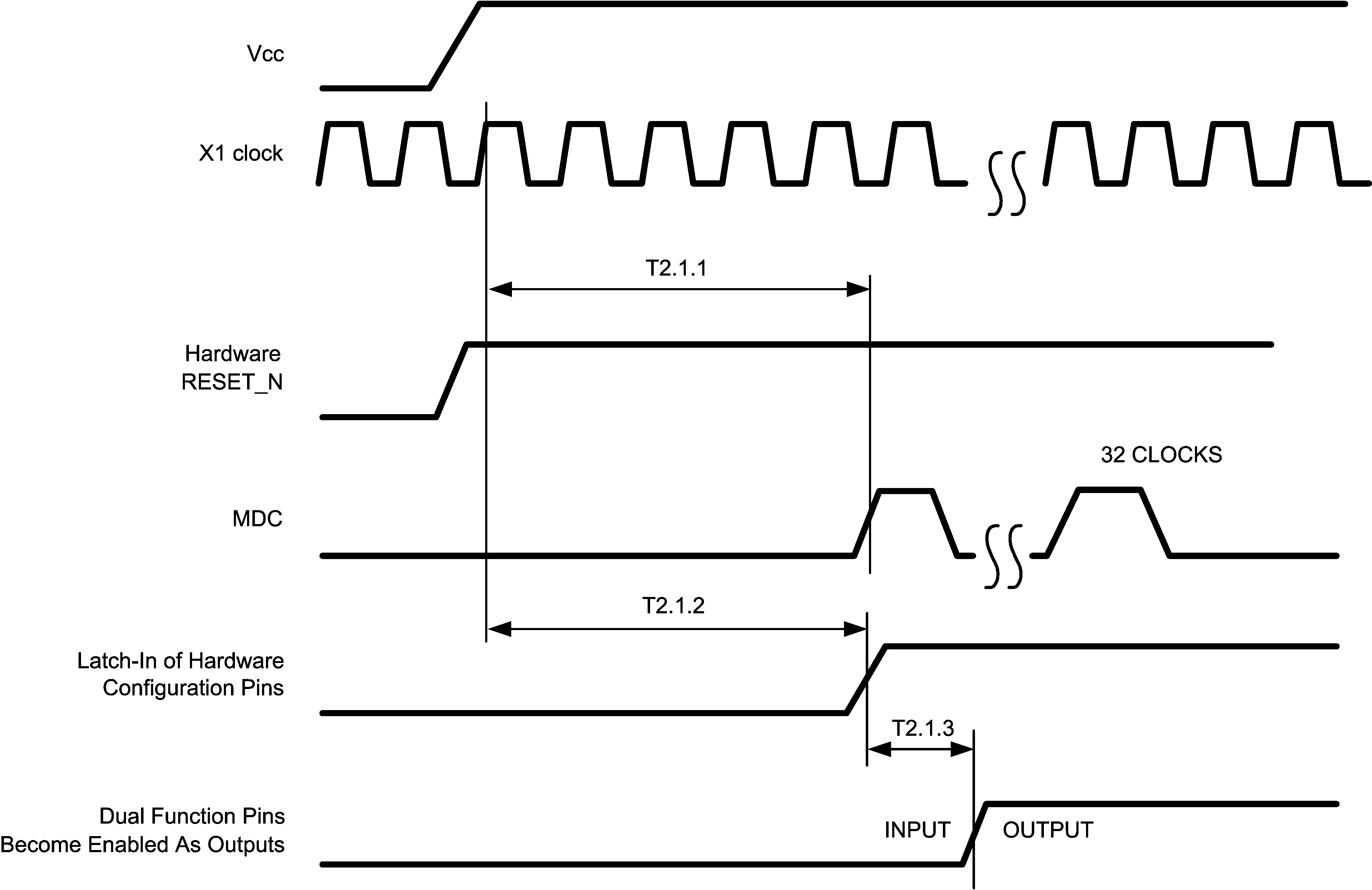 Figure 4-1 Power Up Timing
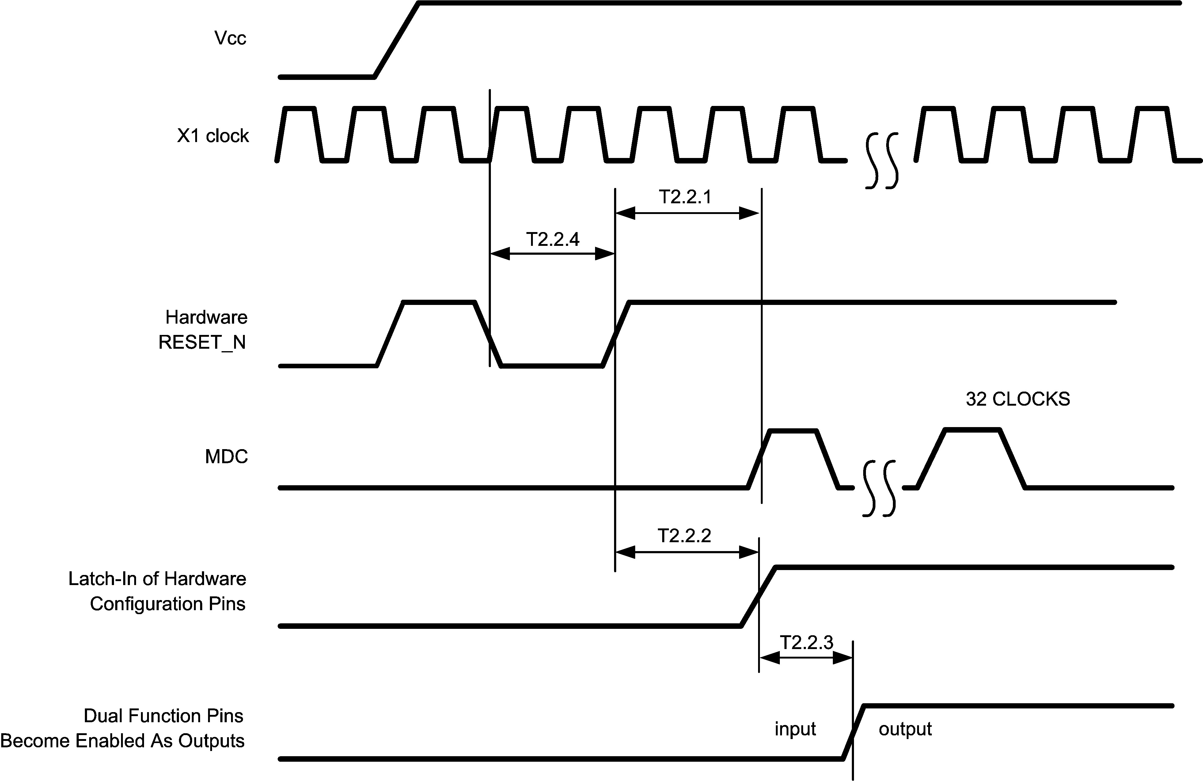 Figure 4-2 Reset Timing
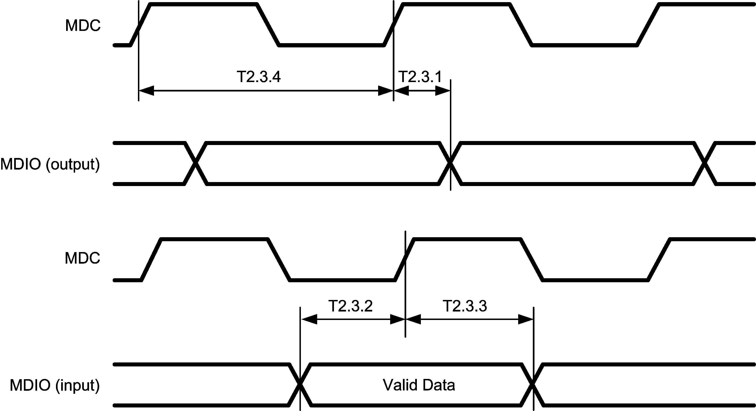 Figure 4-3 MII Serial Management Timing
 Figure 4-4 100 Mb/s MII Transmit Timing
 Figure 4-5 100 Mb/s MII Receive Timing
 Figure 4-6 100BASE-TX MII Transmit Packet Latency Timing
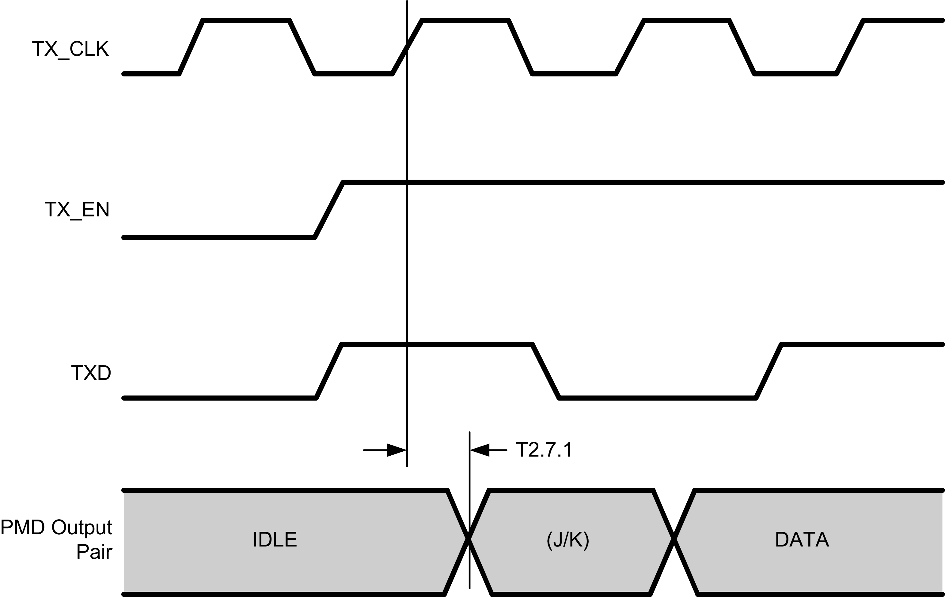 Figure 4-7 100BASE-TX Transmit Packet Deassertion Timing
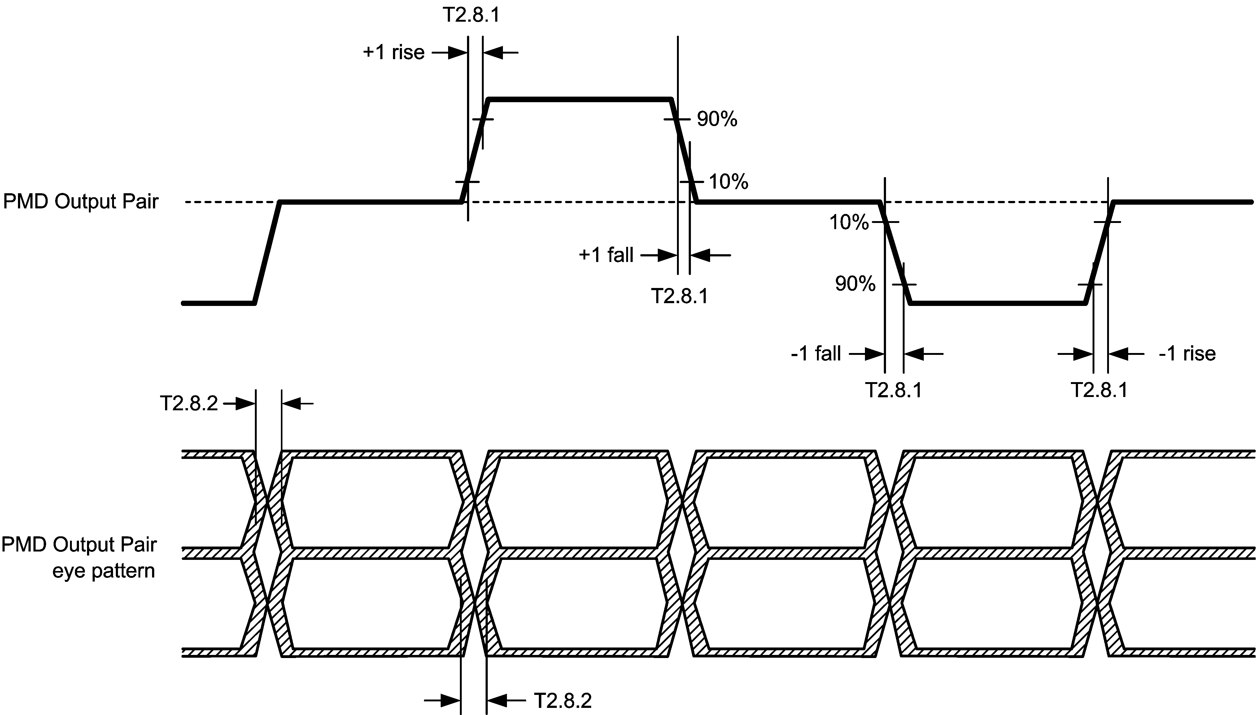 Figure 4-8 100BASE-TX Transmit Timing (tR/F and Jitter)
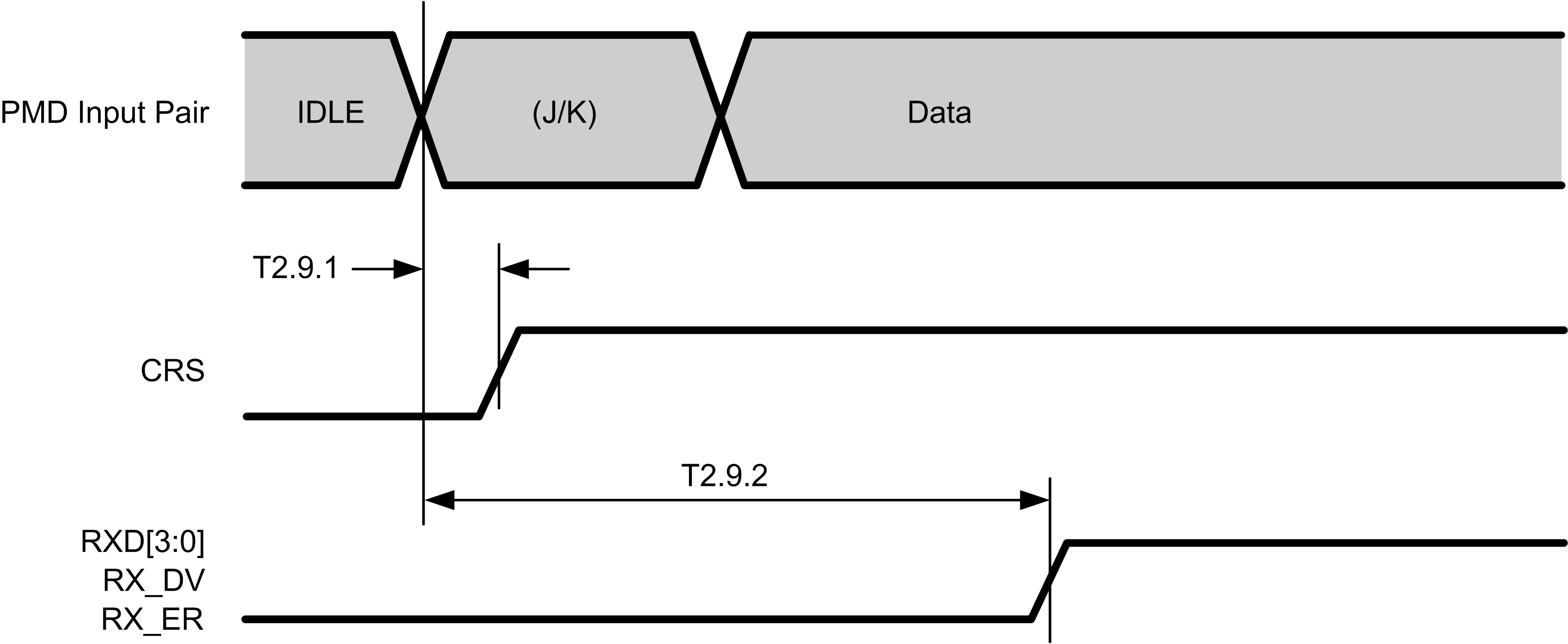 Figure 4-9 100BASE-TX Receive Packet Latency Timing
 Figure 4-10 100BASE-TX Receive Packet Deassertion Timing
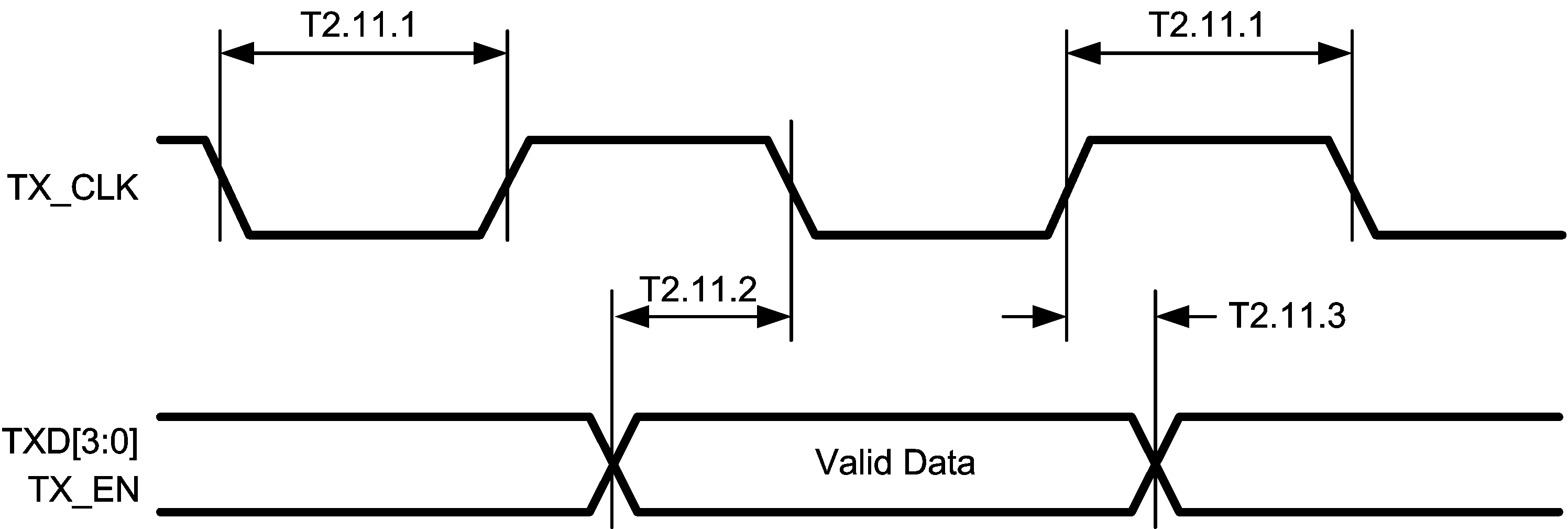 Figure 4-11 10-Mb/s MII Transmit Timing
 Figure 4-12 10-Mb/s MII Receive Timing
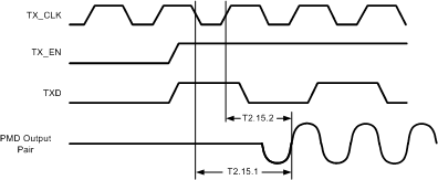 Figure 4-13 10BASE-T Transmit Timing (Start of Packet)
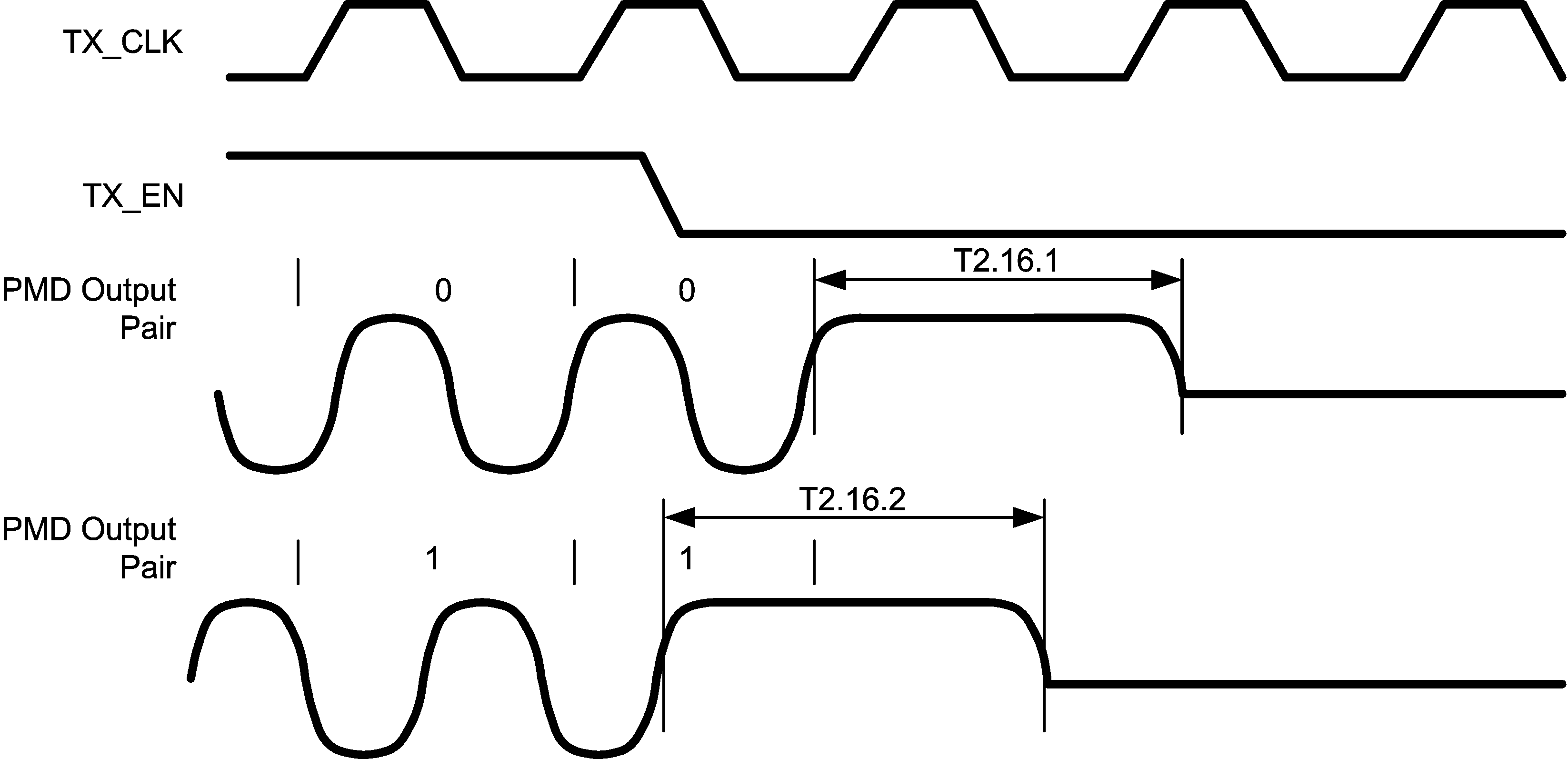 Figure 4-14 10BASE-T Transmit Timing (End of Packet)
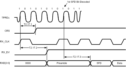 Figure 4-15 10BASE-T Receive Timing (Start of Packet)
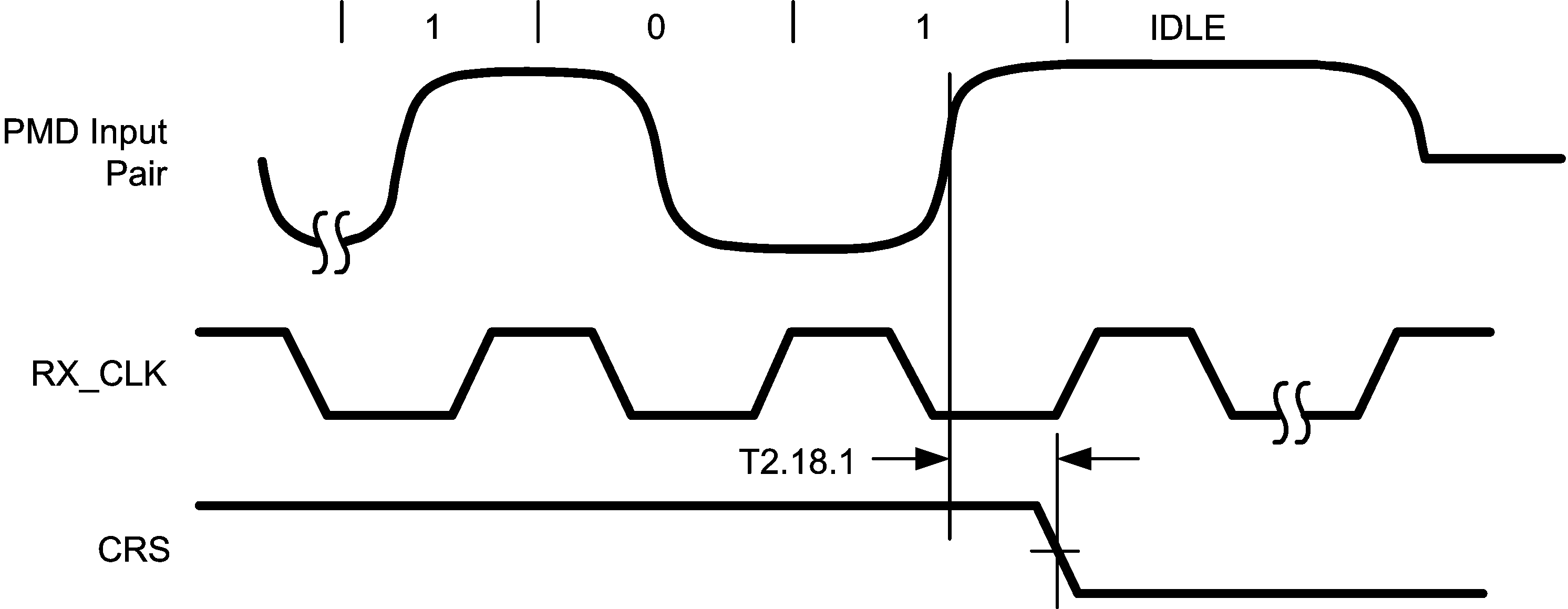 Figure 4-16 10BASE-T Receive Timing (End of Packet)
 Figure 4-17 10-Mb/s Heartbeat Timing
 Figure 4-18 10-Mb/s Jabber Timing
 Figure 4-19 10BASE-T Normal Link Pulse Timing
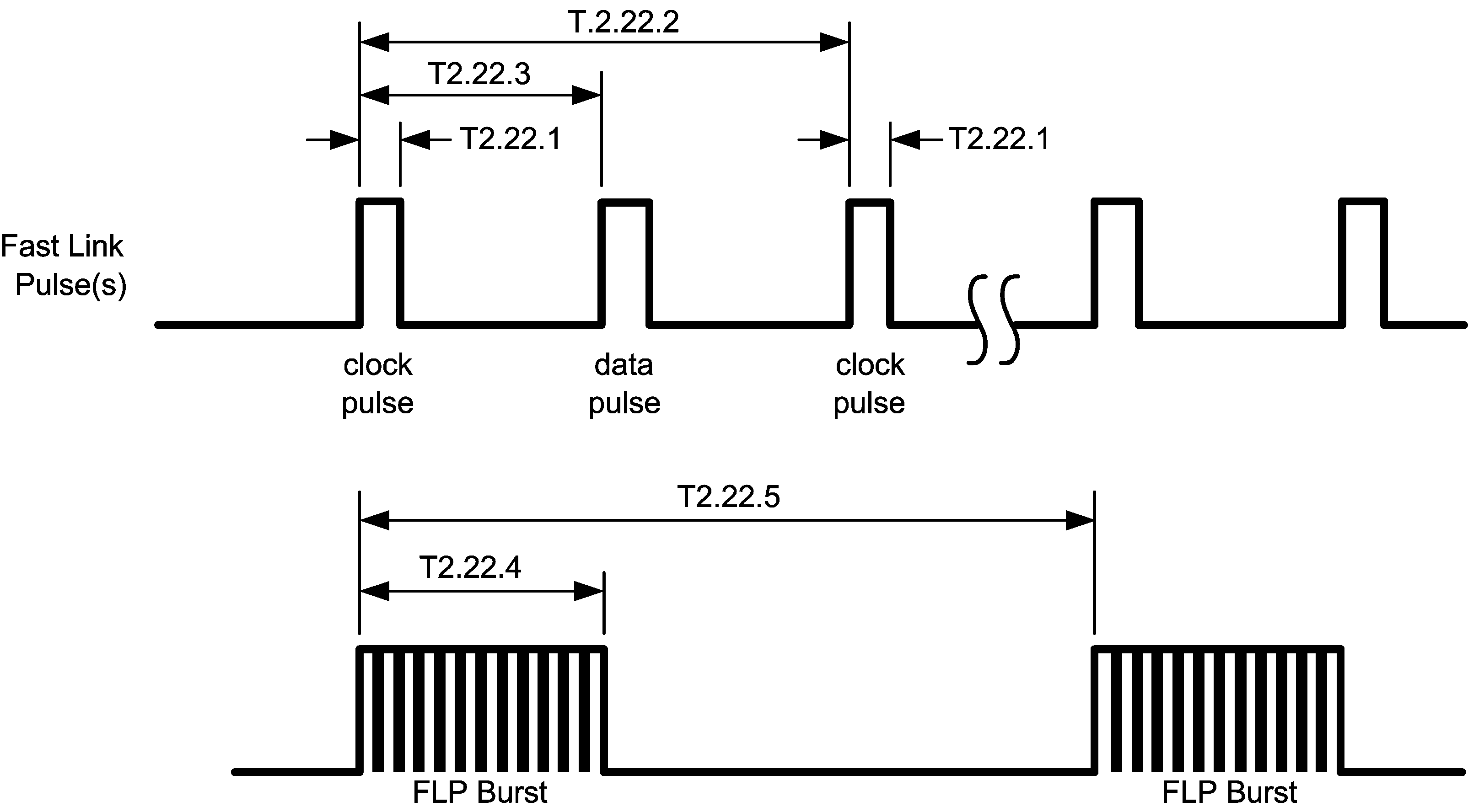 Figure 4-20 Auto-Negotiation Fast Link Pulse (FLP) Timing
 Figure 4-21 100BASE-TX Signal Detect Timing
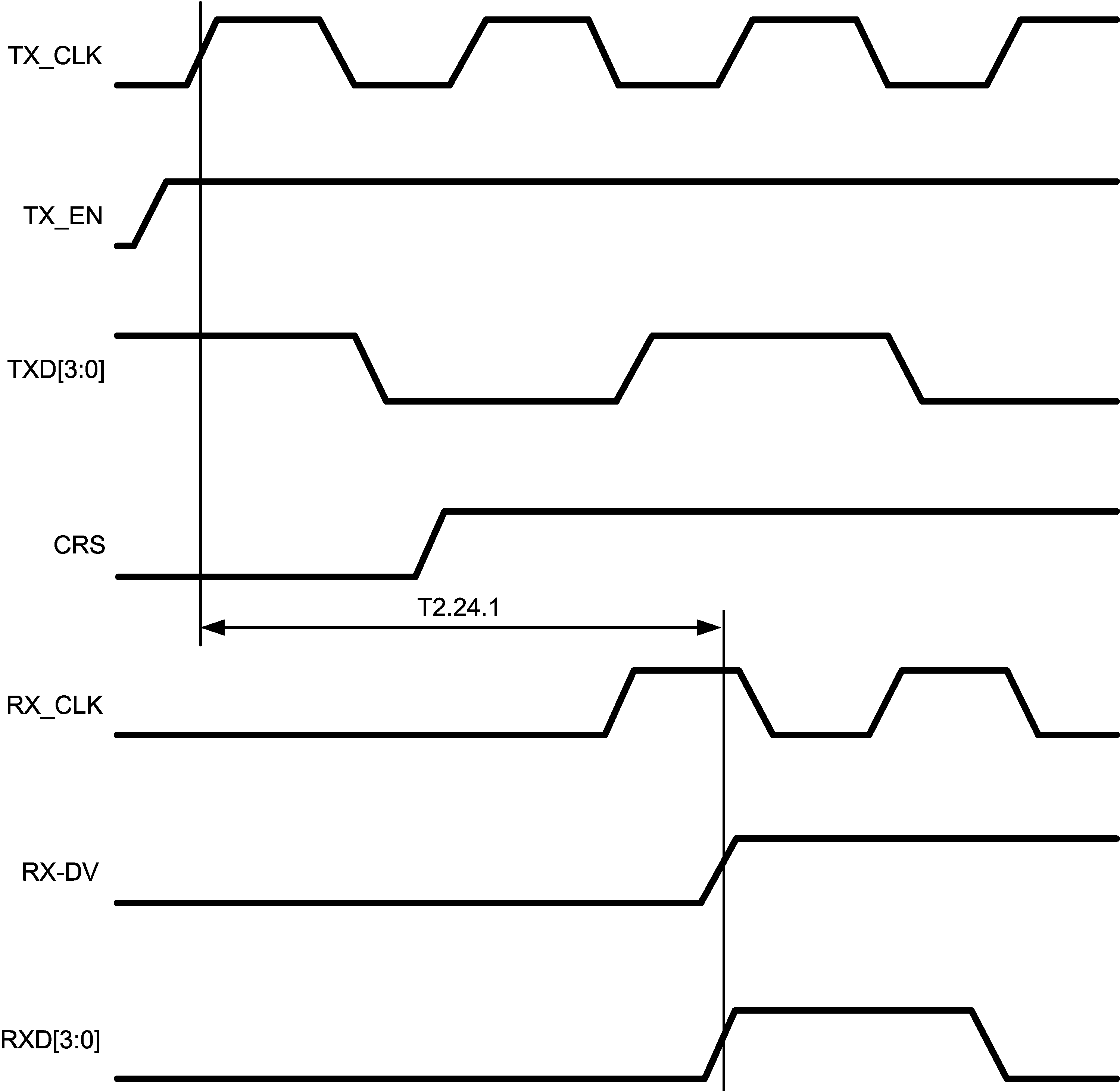 Figure 4-22 100-Mb/s Internal Loopback Timing
 Figure 4-23 10-Mb/s Internal Loopback Timing
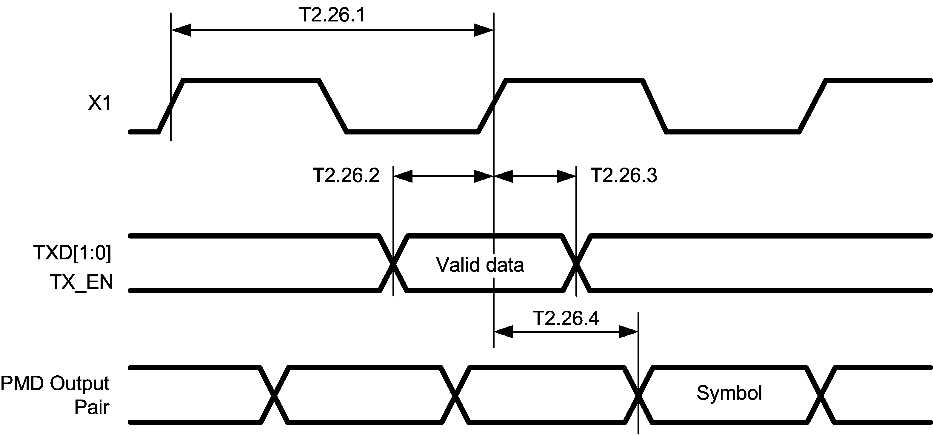 Figure 4-24 RMII Transmit Timing
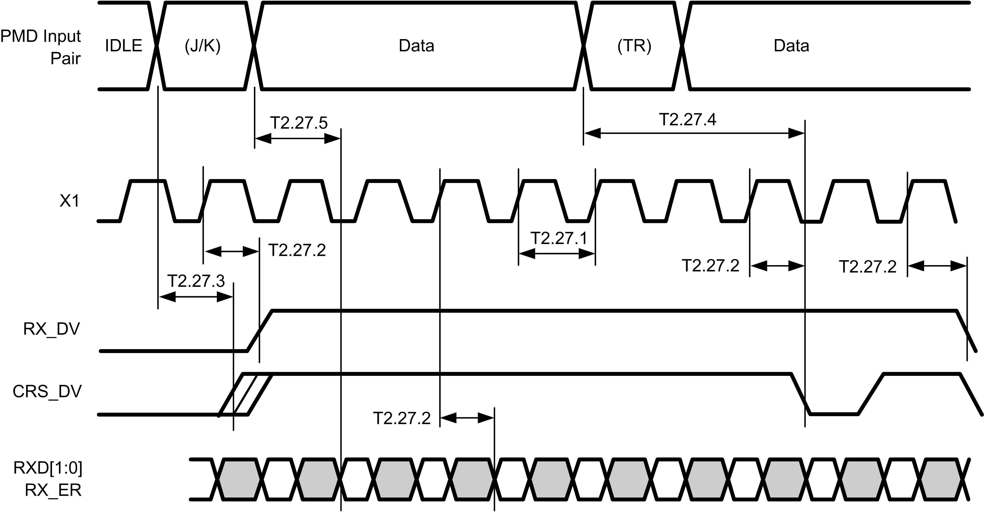 Figure 4-25 RMII Receive Timing
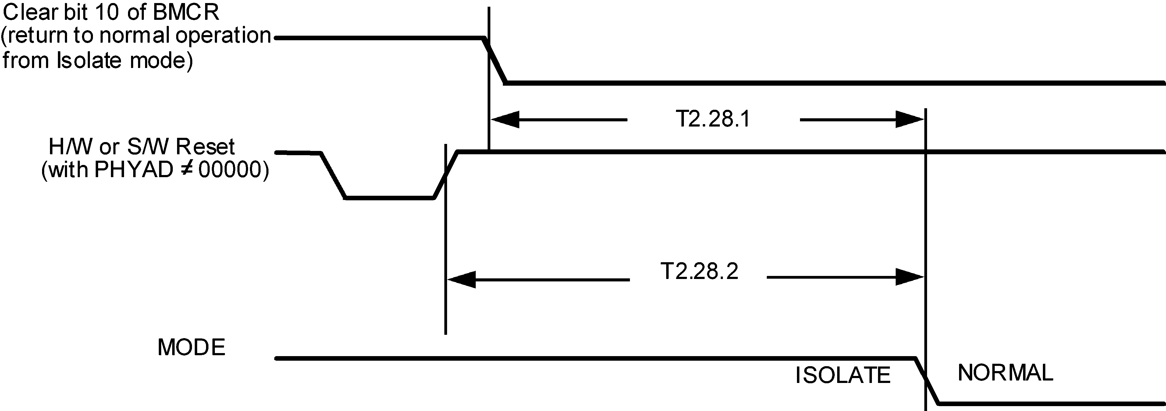 Figure 4-26 Isolation Timing
 Figure 4-27 25 MHz_OUT Timing
 Figure 4-28 100-Mb/s X1 to TX_CLK Timing