SNLS663 December   2021 DP83TC814R-Q1 , DP83TC814S-Q1

PRODUCTION DATA  

  1. Features
  2. Applications
  3. Description
  4. Revision History
  5. Device Comparison Table
  6. Pin Configuration and Functions
  7. Specifications
    1. 7.1 Absolute Maximum Ratings
    2. 7.2 ESD Ratings
    3. 7.3 Recommended Operating Conditions
    4. 7.4 Thermal Information
    5. 7.5 Electrical Characteristics
    6. 7.6 Timing Requirements
    7. 7.7 Timing Diagrams
    8. 7.8 Typical Characteristics
  8. Detailed Description
    1. 8.1 Overview
    2. 8.2 Functional Block Diagram
    3. 8.3 Feature Description
      1. 8.3.1 Diagnostic Tool Kit
        1. 8.3.1.1 Signal Quality Indicator
        2. 8.3.1.2 Electrostatic Discharge Sensing
        3. 8.3.1.3 Time Domain Reflectometry
        4. 8.3.1.4 Voltage Sensing
        5. 8.3.1.5 BIST and Loopback Modes
          1. 8.3.1.5.1 Data Generator and Checker
          2. 8.3.1.5.2 xMII Loopback
          3. 8.3.1.5.3 PCS Loopback
          4. 8.3.1.5.4 Digital Loopback
          5. 8.3.1.5.5 Analog Loopback
          6. 8.3.1.5.6 Reverse Loopback
      2. 8.3.2 Compliance Test Modes
        1. 8.3.2.1 Test Mode 1
        2. 8.3.2.2 Test Mode 2
        3. 8.3.2.3 Test Mode 4
        4. 8.3.2.4 Test Mode 5
    4. 8.4 Device Functional Modes
      1. 8.4.1  Power Down
      2. 8.4.2  Reset
      3. 8.4.3  Standby
      4. 8.4.4  Normal
      5. 8.4.5  Media Dependent Interface
        1. 8.4.5.1 100BASE-T1 Master and 100BASE-T1 Slave Configuration
        2. 8.4.5.2 Auto-Polarity Detection and Correction
        3. 8.4.5.3 Jabber Detection
        4. 8.4.5.4 Interleave Detection
      6. 8.4.6  MAC Interfaces
        1. 8.4.6.1 Media Independent Interface
        2. 8.4.6.2 Reduced Media Independent Interface
        3. 8.4.6.3 Reduced Gigabit Media Independent Interface
      7. 8.4.7  Serial Management Interface
      8. 8.4.8  Direct Register Access
      9. 8.4.9  Extended Register Space Access
      10. 8.4.10 Write Address Operation
        1. 8.4.10.1 MMD1 - Write Address Operation
      11. 8.4.11 Read Address Operation
        1. 8.4.11.1 MMD1 - Read Address Operation
      12. 8.4.12 Write Operation (No Post Increment)
        1. 8.4.12.1 MMD1 - Write Operation (No Post Increment)
      13. 8.4.13 Read Operation (No Post Increment)
        1. 8.4.13.1 MMD1 - Read Operation (No Post Increment)
      14. 8.4.14 Write Operation (Post Increment)
        1. 8.4.14.1 MMD1 - Write Operation (Post Increment)
      15. 8.4.15 Read Operation (Post Increment)
        1. 8.4.15.1 MMD1 - Read Operation (Post Increment)
    5. 8.5 Programming
      1. 8.5.1 Strap Configuration
      2. 8.5.2 LED Configuration
      3. 8.5.3 PHY Address Configuration
    6. 8.6 Register Maps
      1. 8.6.1 Register Access Summary
      2. 8.6.2 DP83TC814 Registers
  9. Application and Implementation
    1. 9.1 Application Information
    2. 9.2 Typical Applications
      1. 9.2.1 Design Requirements
        1. 9.2.1.1 Physical Medium Attachment
          1. 9.2.1.1.1 Common-Mode Choke Recommendations
      2. 9.2.2 Detailed Design Procedure
      3. 9.2.3 Application Curves
  10. 10Power Supply Recommendations
  11. 11Layout
    1. 11.1 Layout Guidelines
      1. 11.1.1 Signal Traces
      2. 11.1.2 Return Path
      3. 11.1.3 Metal Pour
      4. 11.1.4 PCB Layer Stacking
    2. 11.2 Layout Example
  12. 12Device and Documentation Support
    1. 12.1 Receiving Notification of Documentation Updates
    2. 12.2 Support Resources
    3. 12.3 Trademarks
    4. 12.4 Electrostatic Discharge Caution
    5. 12.5 Glossary
  13. 13Mechanical, Packaging, and Orderable Information

Package Options

Mechanical Data (Package|Pins)
Thermal pad, mechanical data (Package|Pins)
Orderable Information

Description

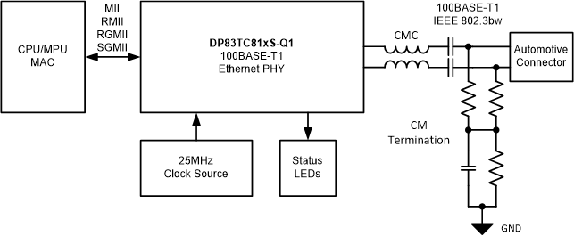
The DP83TC814-Q1 device is an IEEE 802.3bw-compliant automotive PHYTER™ Ethernet physical layer transceiver which can work with Unshielded Twisted Pair cable. It provides all physical layer functions needed to transmit and receive data over unshielded single twisted-pair cables. The device provides xMII flexibility with support for standard MII, RMII, RGMII, and SGMII MAC interfaces.The PHY also integrates a low pass filter on the MDI side to reduce emissions.

This device includes the Diagnostic Tool Kit, providing an extensive list of real-time monitoring tools, debug tools and test modes. Within the tool kit is the first integrated electrostatic discharge (ESD) monitoring tool. It is capable of counting ESD events on MDI as well as providing real-time monitoring through the use of a programmable interrupt. Additionally, the DP83TC814S-Q1includes a pseudo random binary sequence (PRBS) frame generation tool, which is fully compatible with internal loopbacks, to transmit and receive data without the use of a MAC. The device is housed in a 6.00-mm × 6.00-mm, 36-pin VQFN wettable flank package. This device is pin-2-pin compatible with DP83TG720 (1000BASE-T1). It is also form factor compatible with DP83TC811. This would allow for a single PCB layout to be used for DP83TC811, DP83TC812, DP83TC814, and DP83TG720.

Device Information
PART NUMBER PACKAGE (1) BODY SIZE (NOM)
DP83TC814S-Q1 VQFN (36) 6.00 mm × 6.00 mm
DP83TC814R-Q1 VQFN (36) 6.00 mm × 6.00 mm
For all available packages, see the orderable addendum at the end of the data sheet.
GUID-20200818-CA0I-77MC-PRD1-W1NWDVBXP48S-low.gifSimplified Schematic