SNLS604E September   2020  – November 2022 DP83TG720S-Q1

PRODUCTION DATA  

  1. Features
  2. Applications
  3. Description
  4. Revision History
  5. Pin Configuration and Functions
    1.     Pin Functions
    2. 5.1 Pin States
    3. 5.2 Pin Power Domain
  6. Specifications
    1. 6.1 Absolute Maximum Ratings
    2. 6.2 ESD Ratings
    3. 6.3 Recommended Operating Conditions
    4. 6.4 Thermal Information
    5. 6.5 Electrical Characteristics
    6. 6.6 Timing Requirements
    7. 6.7 Timing Diagrams
    8. 6.8 LED Drive Characteristics
  7. Detailed Description
    1. 7.1 Overview
    2. 7.2 Functional Block Diagram
    3. 7.3 Feature Description
      1. 7.3.1 Diagnostic Tool Kit
        1. 7.3.1.1 Signal Quality Indicator
        2. 7.3.1.2 Time Domain Reflectometry
        3. 7.3.1.3 Built-In Self-Test For Datapath
          1. 7.3.1.3.1 Loopback Modes
          2. 7.3.1.3.2 Data Generator
          3. 7.3.1.3.3 Programming Datapath BIST
        4. 7.3.1.4 Temperature and Voltage Sensing
        5. 7.3.1.5 Electrostatic Discharge Sensing
      2. 7.3.2 Compliance Test Modes
        1. 7.3.2.1 Test Mode 1
        2. 7.3.2.2 Test Mode 2
        3. 7.3.2.3 Test Mode 4
        4. 7.3.2.4 Test Mode 5
        5. 7.3.2.5 Test Mode 6
        6. 7.3.2.6 Test Mode 7
    4. 7.4 Device Functional Modes
      1. 7.4.1  Power Down
      2. 7.4.2  Reset
      3. 7.4.3  Standby
      4. 7.4.4  Normal
      5. 7.4.5  Sleep
      6. 7.4.6  State Transitions
        1. 7.4.6.1 State Transition #1 - Standby to Normal
        2. 7.4.6.2 State Transition #2 - Normal to Standby
        3. 7.4.6.3 State Transition #3 - Normal to Sleep
        4. 7.4.6.4 State Transition #4 - Sleep to Normal
      7. 7.4.7  Media Dependent Interface
        1. 7.4.7.1 MDI Master and MDI Slave Configuration
        2. 7.4.7.2 Auto-Polarity Detection and Correction
      8. 7.4.8  MAC Interfaces
        1. 7.4.8.1 Reduced Gigabit Media Independent Interface
        2. 7.4.8.2 Serial Gigabit Media Independent Interface
      9. 7.4.9  Serial Management Interface
      10. 7.4.10 Direct Register Access
      11. 7.4.11 Extended Register Space Access
      12. 7.4.12 Write Address Operation
        1. 7.4.12.1 Example - Write Address Operation
      13. 7.4.13 Read Address Operation
        1. 7.4.13.1 Example - Read Address Operation
      14. 7.4.14 Write Operation (No Post Increment)
        1. 7.4.14.1 Example - Write Operation (No Post Increment)
      15. 7.4.15 Read Operation (No Post Increment)
        1. 7.4.15.1 Example - Read Operation (No Post Increment)
      16. 7.4.16 Write Operation (Post Increment)
        1. 7.4.16.1 Example - Write Operation (Post Increment)
      17. 7.4.17 Read Operation (Post Increment)
        1. 7.4.17.1 Example - Read Operation (Post Increment)
    5. 7.5 Programming
      1. 7.5.1 Strap Configuration
      2. 7.5.2 LED Configuration
      3. 7.5.3 PHY Address Configuration
    6. 7.6 Register Maps
      1. 7.6.1 Register Access Summary
      2. 7.6.2 DP83TG720 Registers
        1. 7.6.2.1 Base Registers
  8. Application and Implementation
    1. 8.1 Application Information
    2. 8.2 Typical Applications
  9. Power Supply Recommendations
  10. 10Compatibility with TI's 100BT1 PHY
  11. 11Layout
    1. 11.1 Layout Guidelines
      1. 11.1.1 Signal Traces
      2. 11.1.2 Return Path
      3. 11.1.3 Physical Medium Attachment
      4. 11.1.4 Metal Pour
      5. 11.1.5 PCB Layer Stacking
  12. 12Device and Documentation Support
    1. 12.1 Receiving Notification of Documentation Updates
    2. 12.2 Support Resources
    3. 12.3 Trademarks
    4. 12.4 Electrostatic Discharge Caution
    5. 12.5 Glossary
  13. 13Mechanical, Packaging, and Orderable Information
    1. 13.1 Package Option Addendum
      1. 13.1.1 Packaging Information
      2. 13.1.2 Tape and Reel Information

Package Options

Mechanical Data (Package|Pins)
Thermal pad, mechanical data (Package|Pins)
Orderable Information

Signal Traces

PCB traces are lossy and long traces can degrade signal quality. Traces should be kept short as possible. Unless mentioned otherwise, all signal traces should be 50-Ω, single-ended impedance. Differential traces should be 50-Ω single-ended and 100-Ω differential. Take care to ensure impedance is controlled throughout. Impedance discontinuities will cause reflections leading to emissions and signal integrity issues. Stubs should be avoided on all signal traces, especially differential signal pairs.
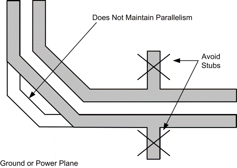
GUID-A799ACCB-18DA-4D5B-88A4-45871D43B313-low.pngFigure 11-1 Differential Signal Trace Routing

Within the differential pairs, trace lengths should be run parallel to each other and matched in length. Matched lengths minimize delay differences, avoiding an increase in common mode noise and emissions. Length matching is also important for MAC interface connections. All transmit signal traces should be length matched to each other and all receive signal traces should be length matched to each other.

Ideally, there should be no crossover or vias on signal path traces. Vias present impedance discontinuities and should be minimized when possible. Route trace pairs on the same layer. Signals on different layers should not cross each other without at least one return path plane between them. Differential pairs should always have a constant coupling distance between them. For convenience and efficiency, TI recommends routing critical signals first (that is, MDI differential pairs, reference clock, and MAC IF traces).