SNLS604E September   2020  – November 2022 DP83TG720S-Q1

PRODUCTION DATA  

  1. Features
  2. Applications
  3. Description
  4. Revision History
  5. Pin Configuration and Functions
    1.     Pin Functions
    2. 5.1 Pin States
    3. 5.2 Pin Power Domain
  6. Specifications
    1. 6.1 Absolute Maximum Ratings
    2. 6.2 ESD Ratings
    3. 6.3 Recommended Operating Conditions
    4. 6.4 Thermal Information
    5. 6.5 Electrical Characteristics
    6. 6.6 Timing Requirements
    7. 6.7 Timing Diagrams
    8. 6.8 LED Drive Characteristics
  7. Detailed Description
    1. 7.1 Overview
    2. 7.2 Functional Block Diagram
    3. 7.3 Feature Description
      1. 7.3.1 Diagnostic Tool Kit
        1. 7.3.1.1 Signal Quality Indicator
        2. 7.3.1.2 Time Domain Reflectometry
        3. 7.3.1.3 Built-In Self-Test For Datapath
          1. 7.3.1.3.1 Loopback Modes
          2. 7.3.1.3.2 Data Generator
          3. 7.3.1.3.3 Programming Datapath BIST
        4. 7.3.1.4 Temperature and Voltage Sensing
        5. 7.3.1.5 Electrostatic Discharge Sensing
      2. 7.3.2 Compliance Test Modes
        1. 7.3.2.1 Test Mode 1
        2. 7.3.2.2 Test Mode 2
        3. 7.3.2.3 Test Mode 4
        4. 7.3.2.4 Test Mode 5
        5. 7.3.2.5 Test Mode 6
        6. 7.3.2.6 Test Mode 7
    4. 7.4 Device Functional Modes
      1. 7.4.1  Power Down
      2. 7.4.2  Reset
      3. 7.4.3  Standby
      4. 7.4.4  Normal
      5. 7.4.5  Sleep
      6. 7.4.6  State Transitions
        1. 7.4.6.1 State Transition #1 - Standby to Normal
        2. 7.4.6.2 State Transition #2 - Normal to Standby
        3. 7.4.6.3 State Transition #3 - Normal to Sleep
        4. 7.4.6.4 State Transition #4 - Sleep to Normal
      7. 7.4.7  Media Dependent Interface
        1. 7.4.7.1 MDI Master and MDI Slave Configuration
        2. 7.4.7.2 Auto-Polarity Detection and Correction
      8. 7.4.8  MAC Interfaces
        1. 7.4.8.1 Reduced Gigabit Media Independent Interface
        2. 7.4.8.2 Serial Gigabit Media Independent Interface
      9. 7.4.9  Serial Management Interface
      10. 7.4.10 Direct Register Access
      11. 7.4.11 Extended Register Space Access
      12. 7.4.12 Write Address Operation
        1. 7.4.12.1 Example - Write Address Operation
      13. 7.4.13 Read Address Operation
        1. 7.4.13.1 Example - Read Address Operation
      14. 7.4.14 Write Operation (No Post Increment)
        1. 7.4.14.1 Example - Write Operation (No Post Increment)
      15. 7.4.15 Read Operation (No Post Increment)
        1. 7.4.15.1 Example - Read Operation (No Post Increment)
      16. 7.4.16 Write Operation (Post Increment)
        1. 7.4.16.1 Example - Write Operation (Post Increment)
      17. 7.4.17 Read Operation (Post Increment)
        1. 7.4.17.1 Example - Read Operation (Post Increment)
    5. 7.5 Programming
      1. 7.5.1 Strap Configuration
      2. 7.5.2 LED Configuration
      3. 7.5.3 PHY Address Configuration
    6. 7.6 Register Maps
      1. 7.6.1 Register Access Summary
      2. 7.6.2 DP83TG720 Registers
        1. 7.6.2.1 Base Registers
  8. Application and Implementation
    1. 8.1 Application Information
    2. 8.2 Typical Applications
  9. Power Supply Recommendations
  10. 10Compatibility with TI's 100BT1 PHY
  11. 11Layout
    1. 11.1 Layout Guidelines
      1. 11.1.1 Signal Traces
      2. 11.1.2 Return Path
      3. 11.1.3 Physical Medium Attachment
      4. 11.1.4 Metal Pour
      5. 11.1.5 PCB Layer Stacking
  12. 12Device and Documentation Support
    1. 12.1 Receiving Notification of Documentation Updates
    2. 12.2 Support Resources
    3. 12.3 Trademarks
    4. 12.4 Electrostatic Discharge Caution
    5. 12.5 Glossary
  13. 13Mechanical, Packaging, and Orderable Information
    1. 13.1 Package Option Addendum
      1. 13.1.1 Packaging Information
      2. 13.1.2 Tape and Reel Information

Package Options

Mechanical Data (Package|Pins)
Thermal pad, mechanical data (Package|Pins)
Orderable Information

Timing Diagrams

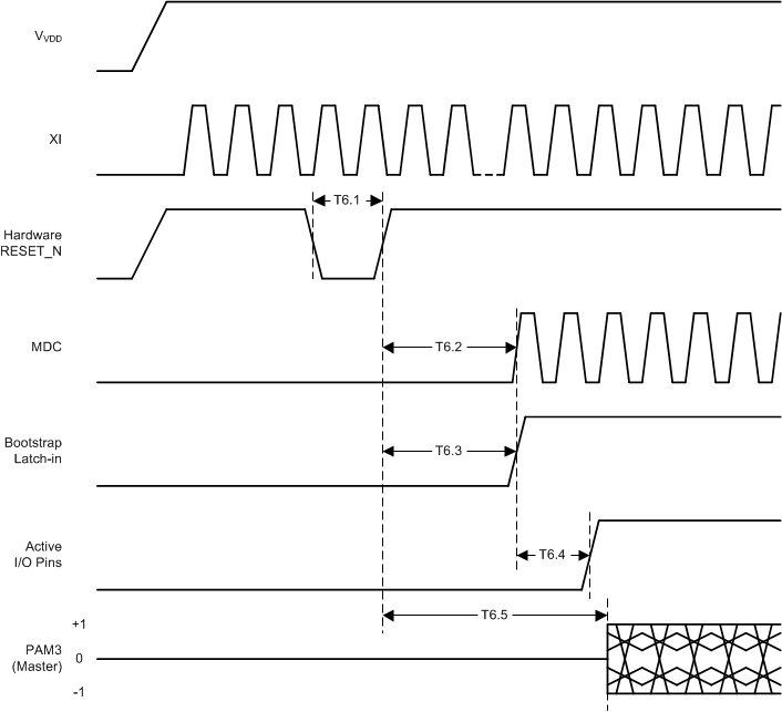
GUID-20200910-CA0I-TGPM-CJGZ-9PC5CQ8BNDZL-low.gif Figure 6-1 Power Up Timing

GUID-D1861084-F5C7-4D1C-BB5D-1FE1F5175E17-low.gifFigure 6-2 Reset Timing
GUID-20200911-CA0I-NCTW-0NMS-MSHMJVFPV049-low.gifFigure 6-3 RGMII Transmit Timing (Internal Delay Enabled)
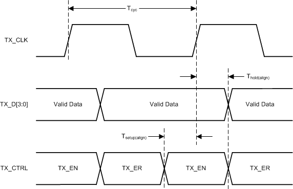
GUID-B75608F0-BC74-4820-AEE9-2E6FA2FF7BA1-low.gifFigure 6-4 RGMII Transmit Timing (Internal Delay Disabled)
GUID-B42F3912-8921-4E03-BC19-86365C100FA3-low.gifFigure 6-5 RGMII Receive Timing (Internal Delay Enabled)
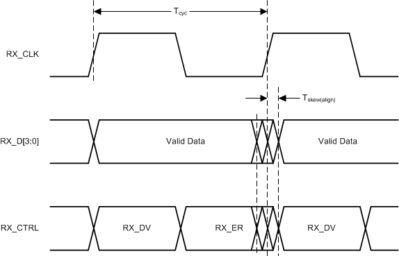
GUID-175AADD9-4813-4536-A437-AD68991A065A-low.gifFigure 6-6 RGMII Receive Timing (Internal Delay Disabled)
GUID-FF8C9414-B1A5-4703-849E-30E642095550-low.gifFigure 6-7 Serial Management Timing