SNLS604E September 2020 – November 2022 DP83TG720S-Q1
PRODUCTION DATA
- 1 Features
- 2 Applications
- 3 Description
- 4 Revision History
- 5 Pin Configuration and Functions
- 6 Specifications
-
7 Detailed Description
- 7.1 Overview
- 7.2 Functional Block Diagram
- 7.3 Feature Description
- 7.4
Device Functional Modes
- 7.4.1 Power Down
- 7.4.2 Reset
- 7.4.3 Standby
- 7.4.4 Normal
- 7.4.5 Sleep
- 7.4.6 State Transitions
- 7.4.7 Media Dependent Interface
- 7.4.8 MAC Interfaces
- 7.4.9 Serial Management Interface
- 7.4.10 Direct Register Access
- 7.4.11 Extended Register Space Access
- 7.4.12 Write Address Operation
- 7.4.13 Read Address Operation
- 7.4.14 Write Operation (No Post Increment)
- 7.4.15 Read Operation (No Post Increment)
- 7.4.16 Write Operation (Post Increment)
- 7.4.17 Read Operation (Post Increment)
- 7.5 Programming
- 7.6 Register Maps
- 8 Application and Implementation
- 9 Power Supply Recommendations
- 10Compatibility with TI's 100BT1 PHY
- 11Layout
- 12Device and Documentation Support
- 13Mechanical, Packaging, and Orderable Information
Package Options
Mechanical Data (Package|Pins)
- RHA|36
Thermal pad, mechanical data (Package|Pins)
- RHA|36
Orderable Information
7.4.8.1 Reduced Gigabit Media Independent Interface
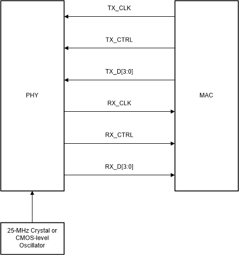
The DP83TG720S-Q1 also supports Reduced Gigabit Media Independent Interface (RGMII) as specified by RGMII version 2.0. RGMII is designed to reduce the number of pins required to connect MAC and PHY. To accomplish this goal, the control signals are multiplexed. Both rising and falling edges of the clock are used to sample the control signal pin on transmit and receive paths. For 1-Gbps operation, RX_CLK and TX_CLK operate at 125 MHz.
The RGMII signals are summarized in Table 7-9:
| FUNCTION | PINS |
|---|---|
| Data Signals | TX_D[3:0] |
| RX_D[3:0] | |
| Control Signals | TX_CTRL |
| RX_CTRL | |
| Clock Signals | TX_CLK |
| RX_CLK |
 Figure 7-13 RGMII Connections
| TX_CTRL (POSITIVE EDGE) | TX_CTRL (NEGATIVE EDGE) | TX_D[3:0] | DESCRIPTION |
|---|---|---|---|
| 0 | 0 | 0000 through 1111 | Normal Inter-Frame |
| 0 | 1 | 0000 through 1111 | Reserved |
| 1 | 0 | 0000 through 1111 | Normal Data Transmission |
| 1 | 1 | 0000 through 1111 | Transmit Error Propagation |
| RX_CTRL (POSITIVE EDGE) | RX_CTRL (NEGATIVE EDGE) | RX_D[3:0] | DESCRIPTION |
|---|---|---|---|
| 0 | 0 | 0000 through 1111 | Normal Inter-Frame |
| 0 | 1 | 0000 through 1101 | Reserved |
| 0 | 1 | 1110 | False Carrier Indication |
| 0 | 1 | 1111 | Reserved |
| 1 | 0 | 0000 through 1111 | Normal Data Reception |
| 1 | 1 | 0000 through 1111 | Data Reception with Errors |
The DP83TG720S-Q1 supports in-band status indication to help simplify link status detection. Inter-frame signals on RX_D[3:0] pins as specified in Table 7-12.
| RX_CTRL | RX_D3 | RX_D[2:1] | RX_D0 |
|---|---|---|---|
| 0
Note: In-band status is only valid when RX_CTRL is low | Duplex Status: 0 = Half-Duplex 1 = Full-Duplex | RX_CLK Clock Speed: 00 = 2.5 MHz 01 = 25 MHz 10 = 125 MHz 11 = Reserved | Link Status: 0 = Link not established 1 = Valid link established |
RGMII MAC Interface for Gigabit Ethernet has stringent timing requirements to meet system level performance. To meet these timing requirements and to operate with different MACs over RGMII, it is advised to take the following requirements into consideration when designing PCB. It is also recommended to check board level signal integrity by using the DP83TG720 IBIS model.
RGMII-TX Requirements
- RGMII TX signals should be routed on board with control impedance of 50Ohm +/-15%.
- Max routing length should be limited to 5inch for better signal integrity performance.
- Figure 7-14 shows a RGMII interface requirements for TX* signals. MAC RGMII driver output impedance should be 50Ohm+/-20%.
- Skew for all RGMII TX signals at TP2, in Figure 7-14, should be <±500ps.
- Signal Integrity at TP1 and TP2, in Figure 7-14, should be verified with IBIS model simulation and ensured conformance to following requirements:
- At TP2, signal should meet rise/fall time of 1ns (20-80%) of signal amplitude.
- Rise/fall time should be monotonic between VIH/VIL level at TP2.
 Figure 7-14 RGMII TX Requirements
RGMII-RX Requirements
- RGMII RX signals should be routed on board with control impedance of 50Ohm +/-15%.
- Max routing length should be limited to 5inch for better signal integrity performance.
- No damping resistors should be added at TP3/TP4, in Figure 7-15, as that will impact signal integrity of RX signals.
- Figure 7-15 shows a RGMII interface requirements for RX* signals. MAC RGMII driver output impedance should be 50Ohm+/-20%.
- Signal Integrity at TP3 and TP4, in Figure 7-15, should be verified with IBIS model simulation and ensured conformance to following requirements:
- At TP4, signal should meet rise/fall time of 1ns (20-80%) of signal amplitude.
- Rise/fall time should be monotonic between VIH/VIL level at TP4.
 Figure 7-15 RGMII RX Requirements
- We recommend routing RGMII on buried traces to minimize EMC emissions.
- Buried traces should be connected with via placement as close as possible to the PHY and MAC.