SNLS604E September 2020 – November 2022 DP83TG720S-Q1
PRODUCTION DATA
- 1 Features
- 2 Applications
- 3 Description
- 4 Revision History
- 5 Pin Configuration and Functions
- 6 Specifications
-
7 Detailed Description
- 7.1 Overview
- 7.2 Functional Block Diagram
- 7.3 Feature Description
- 7.4
Device Functional Modes
- 7.4.1 Power Down
- 7.4.2 Reset
- 7.4.3 Standby
- 7.4.4 Normal
- 7.4.5 Sleep
- 7.4.6 State Transitions
- 7.4.7 Media Dependent Interface
- 7.4.8 MAC Interfaces
- 7.4.9 Serial Management Interface
- 7.4.10 Direct Register Access
- 7.4.11 Extended Register Space Access
- 7.4.12 Write Address Operation
- 7.4.13 Read Address Operation
- 7.4.14 Write Operation (No Post Increment)
- 7.4.15 Read Operation (No Post Increment)
- 7.4.16 Write Operation (Post Increment)
- 7.4.17 Read Operation (Post Increment)
- 7.5 Programming
- 7.6 Register Maps
- 8 Application and Implementation
- 9 Power Supply Recommendations
- 10Compatibility with TI's 100BT1 PHY
- 11Layout
- 12Device and Documentation Support
- 13Mechanical, Packaging, and Orderable Information
Package Options
Mechanical Data (Package|Pins)
- RHA|36
Thermal pad, mechanical data (Package|Pins)
- RHA|36
Orderable Information
7.5.1 Strap Configuration
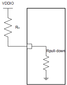
The DP83TG720S-Q1 uses functional pins as strap options to place the device into specific modes of operation. The values of these pins are sampled at power up and hardware reset (through either the RESET_N pin or register access). The strap pins support 2-levels and 3-levels, which are described in greater detail below. Configuration of the device may be done through strapping or through serial management interface.
Note:  Figure 7-18 Strap Circuit
- Because strap pins are functional pins after reset is deasserted, they should not be connected directly to VCC or GND.
- Pull up strap resistors are sufficient to enter different strap modes.
- Pull down strap resistor can have application for LED pin straps. Refer to LED Configuration section.
 Figure 7-18 Strap Circuit
Table 7-16 Recommended 3-level Strap Resistor Ratios
| MODE | IDEAL RH (kΩ)1
for VDDIO = 3.3 V | IDEAL RH (kΩ)2
for VDDIO = 2.5 V | IDEAL RH (kΩ)1
for VDDIO = 1.8V |
|---|---|---|---|
| 1 | OPEN | OPEN | OPEN |
| 2 | 13 | 12 | 4 |
| 3 | 4.5 | 2 | 0.8 |
- 10% resistor accuracy
- 1% resistor accuracy
- 10% resistor accuracy
- To gain more margin in customer application for 1.8V VDDIO, either 2.1K+/-10% pull-up can be used or resistor accuracy of 2.49K resistor can be limited to 1%.
The following table describes the DP83TG720S-Q1 configuration bootstraps:
Table 7-18 2-level Bootstraps
| PIN NAME | PIN NO. | STRAP MODE | STRAP FUNCTION | DESCRIPTION |
| RX_D0 | 26 | 1 (default) | MAC[0] = 0 | MAC Interface Selection [0]. Refer to Table 7-19 for full description. |
| 2 | MAC[0] = 1 | |||
| RX_D1 | 25 | 1 (default) | MAC[1] = 0 | MAC Interface Selection [1]. Refer to Table 7-19 for full description. |
| 2 | MAC[1] = 1 | |||
| RX_D2 | 24 | 1 (default) | MAC[2] = 0 | MAC Interface Selection [2]. Refer to Table 7-19 for full description. |
| 2 | MAC[2] = 1 | |||
| LED_0 | 1 | 1 (default) | MS = 0 | MDI Master Slave Select. MS = 0 Slave MS = 1 Master |
| 2 | MS = 1 | |||
| LED_1 | 6 | 1 (default) | AUTO = 0 | Autonomous Disable AUTO = 0 Autonomous AUTO = 1 Managed |
| 2 | AUTO = 1 |
Table 7-19 MAC Interface Selection Bootstraps
| MAC[2] | MAC[1] | MAC[0] | DESCRIPTION |
|---|---|---|---|
| 0 | 0 | 0 | SGMII (4-wire) |
| 0 | 0 | 1 | RESERVED |
| 0 | 1 | 0 | RESERVED |
| 0 | 1 | 1 | RESERVED |
| 1 | 0 | 0 | RGMII (Align Mode) |
| 1 | 0 | 1 | RGMII (TX Shift Mode) |
| 1 | 1 | 0 | RGMII (TX and RX Shift Mode) |
| 1 | 1 | 1 | RGMII (RX Shift Mode) |
Table 7-20 3-Level Bootstrap: PHY Address
| PHY_AD[3:0] | RX_CTRL STRAP MODE | STRP_1 STRAP MODE | DESCRIPTION |
|---|---|---|---|
| 0000 | 1 | 1 | PHY Address: 0x0000 (0) |
| 0001 | - | - | RESERVED |
| 0010 | - | - | RESERVED |
| 0011 | - | - | RESERVED |
| 0100 | 2 | 1 | PHY Address: 0x0004 (4) |
| 0101 | 3 | 1 | PHY Address: 0x0005 (5) |
| 0110 | - | - | RESERVED |
| 0111 | - | - | RESERVED |
| 1000 | 1 | 2 | PHY Address: 0x0008 (8) |
| 1001 | - | - | RESERVED |
| 1010 | 1 | 3 | PHY Address: 0x000A (10) |
| 1011 | - | - | RESERVED |
| 1100 | 2 | 2 | PHY Address: 0x000C (12) |
| 1101 | 3 | 2 | PHY Address: 0x000D (13) |
| 1110 | 2 | 3 | PHY Address: 0x000E (14) |
| 1111 | 3 | 3 | PHY Address: 0x000F (15) |