DRV11873 12-V, 3-Phase, Sensorless BLDC Motor Driver
1 Features
- Input Voltage Range: 5 to 16 V
- Six Integrated MOSFETs With 1.5-A Continuous Output Current
- Total Driver H + L RDSON 450 mΩ
- Sensorless Proprietary BMEF Control Scheme
- 150° Commutation
- Synchronous Rectification PWM Operation
- FG and RD Open-Drain Output
- 5-V LDO for External Use up to 20 mA
- PWMIN Input from 7 to 100 kHz
- Overcurrent Protection With Adjustable Limit Through External Resistor
- Lock Detection
- Voltage Surge Protection
- UVLO
- Thermal Shutdown
2 Applications
- Appliance Cooling Fan
- Desktop Cooling Fan
- Server Cooling Fan
3 Description
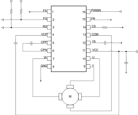
DRV11873 is a three-phase, sensorless motor driver with integrated power MOSFETs with drive current capability up to 1.5-A continuous and 2-A peak. DRV11873 is specifically designed for fan motor drive applications with low noise and low external component count. DRV11873 has built-in overcurrent protection with no external current sense resistor needed. The synchronous rectification mode of operation achieves increased efficiency for motor driver applications. DRV11873 outputs FG and RD to indicate motor status with open-drain output. A 150° sensorless BEMF control scheme is implemented for a three-phase motor. DRV11873 is available in the thermally-efficient 16-pin TSSOP package. The operation temperature is specified from –40°C to 125°C.
Device Information(1)
| PART NUMBER | PACKAGE | BODY SIZE (NOM) |
|---|---|---|
| DRV11873 | HTSSOP (16) | 4.40 mm × 5.00 mm |
- For all available packages, see the orderable addendum at the end of the data sheet.
4 Simplified Schematic
5 Revision History
Changes from * Revision (November 2012) to A Revision
- Added Handling Ratings table, Feature Description section, Device Functional Modes, Application and Implementation section, Power Supply Recommendations section, Layout section, Device and Documentation Support section, and Mechanical, Packaging, and Orderable Information section Go
- Changed ƒPWM minimum valueGo
6 Pin Configuration and Functions
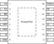
Pin Functions
| PIN | I/O(1) | DESCRIPTION | |
|---|---|---|---|
| NAME | NO. | ||
| FS | 1 | I | Motor parameter adjustment pin. Pull low for lower-speed motor and pull high for high-speed motor. |
| FG | 2 | O | Frequency generator output. The output period is equal to 6 electrical states (FG). |
| RD | 3 | O | In the lock condition, RD output is high through a pullup resistor to VCC or 5 V. |
| VCP | 4 | O | Charge pump output |
| CPP | 5 | O | Charge pump conversion terminal |
| CPN | 6 | O | Charge pump conversion terminal |
| W | 7 | O | Phase W output |
| GND | 8 | — | Ground pin |
| V | 9 | O | Phase V output |
| U | 10 | O | Phase U output |
| VCC | 11 | I | Input voltage for motor and chip supply voltage |
| V5 | 12 | O | 5-V regulator output |
| COM | 13 | I | Motor common terminal input. If the motor does not have a common wire, see Application and Implementation for more details. |
| CS | 14 | I | Overcurrent threshold set-up pin. A resistor set-up current limit is connected between this pin and ground. The voltage across the resistor compares with the voltage converted from the bottom MOSFETs' current. If MOSFETs' current is high, the part goes into the overcurrent protection mode by turning off the top PWM MOSFET and keeping the bottom MOSFET on. Ilimit(A) = 6600 / RCS (Ω); Equation valid range: 500 mA < Ilimit < 2000 mA |
| FR | 15 | I | Set high for reverse rotation. Set low or floating for forward rotation. |
| PWMIN | 16 | I | PWM input pin. The PWM input signal is converted to a fixed switching frequency on the MOSFET driver. |
7 Specifications
7.1 Absolute Maximum Ratings
over operating free-air temperature (unless otherwise noted)| MIN | MAX | UNIT | ||
|---|---|---|---|---|
| Input voltage(1) | VCC | –0.3 | 20 | V |
| CS | –0.3 | 3.6 | ||
| PWMIN, FS, FR | –0.3 | 6 | ||
| GND | –0.3 | 0.3 | ||
| COM | –1 | 20 | ||
| Output voltage(1) | U, V, W | –1 | 20 | V |
| FG, RD | –0.3 | 20 | ||
| VCP | –0.3 | 25 | ||
| CPN | –0.3 | 20 | ||
| CPP | –0.3 | 25 | ||
| V5 | –0.3 | 6 | ||
| TJ | Operating junction temperature | –40 | 125 | °C |
7.2 Handling Ratings
| MIN | MAX | UNIT | |||
|---|---|---|---|---|---|
| Tstg | Storage temperature range | –55 | 150 | °C | |
| V(ESD) | Electrostatic discharge | Human body model (HBM), per ANSI/ESDA/JEDEC JS-001, all pins(1) | –4000 | 4000 | V |
| Charged device model (CDM), per JEDEC specification JESD22-C101, all pins(2) | –1000 | 1000 | |||
| Machine model (MM) | –200 | 200 | |||
7.3 Recommended Operating Conditions
over operating free-air temperature range (unless otherwise noted)| MIN | MAX | UNIT | ||
|---|---|---|---|---|
| Supply voltage | VCC | 5 | 16 | V |
| Voltage range | U, V, W | –0.7 | 17 | V |
| COM | –0.1 | 17 | ||
| FG, RD | –0.1 | 16 | ||
| PGND, GND | –0.1 | 0.1 | ||
| VCP | –0.1 | 22 | ||
| CPP | –0.1 | 22 | ||
| CPN | –0.1 | 16 | ||
| V5 | –0.1 | 5.5 | ||
| PWMIN, FR, FS | –0.1 | 5.5 | ||
| TJ | Operating junction temperature | –40 | 125 | V |
7.4 Thermal Information
| THERMAL METRIC(1) | DRV11873 | UNIT | |
|---|---|---|---|
| PWP | |||
| 16 PINS | |||
| RθJA | Junction-to-ambient thermal resistance | 39.4 | °C/W |
| RθJC(top) | Junction-to-case (top) thermal resistance | 30.3 | |
| RθJB | Junction-to-board thermal resistance | 25.6 | |
| ψJT | Junction-to-top characterization parameter | 0.5 | |
| ψJB | Junction-to-board characterization parameter | 10.2 | |
| RθJC(bot) | Junction-to-case (bottom) thermal resistance | 3.6 | |
7.5 Electrical Characteristics
over recommended operating free-air temperature (unless otherwise noted)7.6 Typical Characteristics

| Input voltage = 12 V | PWM duty = 100% | FS = 1 |
| t = 20 ms/div | ||

| Input voltage = 12 V | PWM duty = 100% | FS = 1 |
| t = 800 µs/div | ||

| Input voltage = 12 V | PWM duty = 100% | FS = 1 |
| t = 1 s/div |


| Input voltage = 12 V | PWM duty = 10% | FS = 1 |
| t = 40 ms/div | ||

| Input voltage = 12 V | PWM duty = 50% | FS = 1 |
| t = 800 µs/div | ||

| Input voltage = 12 V | PWM duty switch from 100% to 20% | |
| t = 20 ms/div | FS = 1 | |


