DRV13x Audio-Balanced Line Drivers
1 Features
- Balanced Output
- Low Distortion: 0.0005% at f = 1 kHz
- Wide Output Swing: 17Vrms into 600 Ω
- High Capacitive Load Drive
- High Slew Rate: 15 V/µs
- Wide Supply Range: ±4.5 V to ±18 V
- Low Quiescent Current: ±5.2 mA
- 8-Pin DIP, SO-8, and SOL-16 Packages
- Companion to Audio Differential Line Receivers: INA134 and INA137
- Improved Replacement for SSM2142
2 Applications
- Audio Differential Line Drivers
- Audio Mix Consoles
- Distribution Amplifiers
- Graphic and Parametric Equalizers
- Dynamic Range Processors
- Digital Effects Processors
- Telecom Systems
- Hi-Fi Equipment
- Industrial Instrumentation
3 Description
The DRV134 and DRV135 are differential output amplifiers that convert a single-ended input to a balanced output pair. These balanced audio drivers consist of high performance op amps with on-chip precision resistors. They are fully specified for high performance audio applications and have excellent ac specifications, including low distortion (0.0005% at 1 kHz) and high slew rate (15 V/µs).
The on-chip resistors are laser-trimmed for accurate gain and optimum output common-mode rejection. Wide output voltage swing and high output drive capability allow use in a wide variety of demanding applications. They easily drive the large capacitive loads associated with long audio cables. Used in combination with the INA134 or INA137 differential receivers, they offer a complete solution for transmitting analog audio signals without degradation.
The DRV134 is available in 8-pin DIP and SOL-16 surface-mount packages. The DRV135 comes in a space-saving SO-8 surface-mount package. Both are specified for operation over the extended industrial temperature range, –40°C to +85°C and operate from –55°C to +125°C.
Device Information(1)
| PART NUMBER | PACKAGE | BODY SIZE (NOM) |
|---|---|---|
| DRV134 | SOIC (16) | 10.30 mm × 7.50 mm |
| DRV135 | SOIC (8) | 4.90 mm × 3.91 mm |
- For all available packages, see the orderable addendum at the end of the datasheet.
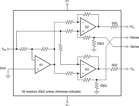
4 Simplified Schematic
5 Revision History
Changes from A Revision (April 2007) to B Revision
- Added Handling Rating table, Feature Description section, Device Functional Modes, Application and Implementation section, Power Supply Recommendations section, Layout section, Device and Documentation Support section, and Mechanical, Packaging, and Orderable Information section Go
6 Pin Configuration and Functions

Pin Functions
| PIN | I/O | DESCRIPTION | ||
|---|---|---|---|---|
| NAME | DIP-8 and SO-8 | SOL-16 | ||
| Gnd | 3 | 5 | – | Ground |
| +Sense | 7 | 13 | I | Sensing, non-inverting input |
| –Sense | 2 | 4 | I | Sensing, inverting input |
| V+ | 6 | 12 | – | Positive supply |
| V– | 5 | 11 | – | Negative supply |
| VIN | 4 | 6 | I | Input |
| –Vo | 1 | 3 | O | Inverted, balanced differential output |
| +Vo | 8 | 14 | O | Balanced differential output |
| NC | – | 1,2,7,8,9,10,15,16 | – | These pins should be left unconnected |
7 Specifications
7.1 Absolute Maximum Ratings
over operating free-air temperature range (unless otherwise noted) (1)| MIN | MAX | UNIT | ||
|---|---|---|---|---|
| Supply voltage, V+ to V– | 40 | V | ||
| Input voltage range | V– | V+ | ||
| Output short-circuit (to ground) | Continuous | |||
| Operating temperature | –55 | 125 | °C | |
| Junction temperature | 150 | °C |
7.2 Handling Ratings
| MIN | MAX | UNIT | |||
|---|---|---|---|---|---|
| Tstg | Storage temperature range | –55 | 125 | °C | |
| V(ESD) | Electrostatic discharge | Human body model (HBM), per ANSI/ESDA/JEDEC JS-001, all pins(1) | –2000 | 2000 | V |
| Charged device model (CDM), per JEDEC specification JESD22-C101, all pins(2) | –500 | 500 | |||
7.3 Recommended Operating Conditions
over operating free-air temperature range (unless otherwise noted)| MIN | NOM | MAX | UNIT | ||
|---|---|---|---|---|---|
| Tspe | Specification temperature range | –40 | 85 | °C | |
| TA | Operation temperature range | –55 | 125 | °C | |
| V+ | Positive supply | 4.5 | 18 | 18 | V |
| V– | Negative supply | –4.5 | –18 | –18 | V |
7.4 Electrical Characteristics
At TA = +25°C, VS = ±18 V, RL = 600 Ω differential connected between +VO and –VO, unless otherwise noted.| PARAMETER | TEST CONDITIONS | MIN | TYP | MAX | UNIT | |||
|---|---|---|---|---|---|---|---|---|
| AUDIO PERFORMANCE | ||||||||
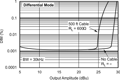
| THD+N | Total Harmonic Distortion + Noise | f = 20Hz to 20kHz, VO = 10Vrms f = 1kHz, VO = 10Vrms 20 kHz BW THD+N < 1% |
0.001% | |||||
| 0.0005% | ||||||||
| RTO(1) | Noise Floor | –98 | dBu | |||||
| RTO(1) | Headroom | 27 | dBu | |||||
| INPUT | ||||||||
| ZIN | Input Impedance(2) | 10 | kΩ | |||||
| IIN | Input Current | VIN = ±7.07 V | –1000 | ±700 | 1000 | µA | ||
| GAIN | ||||||||
| Differential | [(+VO) – (–VO)]/VIN
VIN = ±10V |
|||||||
| Initial | 5.8 | 6 | dB | |||||
| Error | –2% | ±0.1% | 2% | |||||
| Error vs Temperature | ±10 | ppm/°C | ||||||
| Single-Ended | VIN = ±5V | |||||||
| Initial | 5.8 | 6 | dB | |||||
| Error | –2% | ±0.7% | 2% | |||||
| Error vs Temperature | ±10 | ppm/°C | ||||||
| Nonlinearity | 0.0003 | % of FS | ||||||
| OUTPUT | ||||||||
| OCMR | Common-Mode Rejection, f = 1kHz | See Figure 25 | 46 | 68 | dB | |||
| SBR | Signal Balance Ratio, f = 1kHz | See Figure 26 | 35 | 54 | dB | |||
| Output Offset Voltage | ||||||||
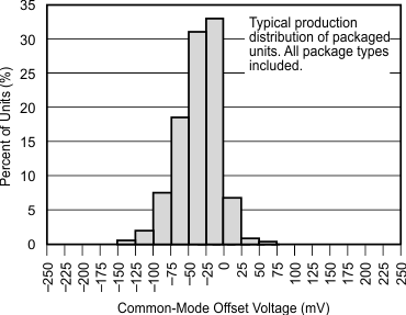
| VOCM(3) | Offset Voltage, Common-Mode | VIN = 0 | –250 | ±50 | 250 | mV | ||
| Offset Voltage, Common-Mode vs Temperature | ±150 | µV/°C | ||||||
| VOD(4) | Offset Voltage, Differential | VIN = 0 | –10 | ±1 | 10 | mV | ||
| Offset Voltage, Differential vs Temperature | ±5 | µV/°C | ||||||
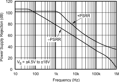
| PSRR | Offset Voltage, Differential vs Power Supply | VS = ±4.5V to ±18V | 80 | 110 | dB | |||
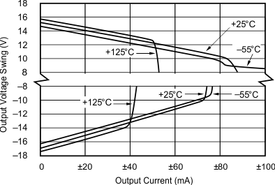
| Output Voltage Swing, | Positive | No Load(5) | (V+) – 3 | (V+) – 2.5 | V | |||
| Negative | (V–) + 2 | (V–) + 1.5 | ||||||
| Impedance | 50 | Ω | ||||||
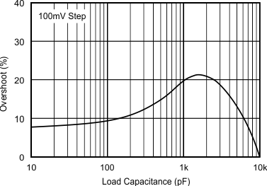
| CL | Load Capacitance, Stable Operation | CL Tied to Ground (each output) | 1 | µF | ||||
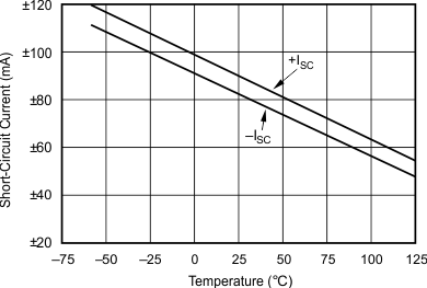
| ISC | Short-Circuit Current | ±85 | mA | |||||
| FREQUENCY RESPONSE | ||||||||
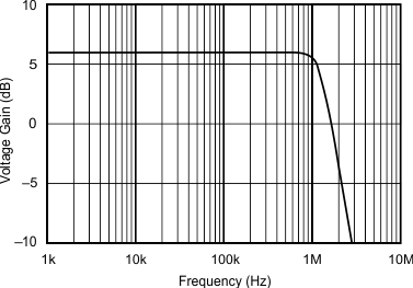
| Small-Signal Bandwidth | 1.5 | MHz | ||||||
| SR | Slew Rate | 15 | V/µs | |||||
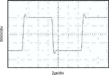
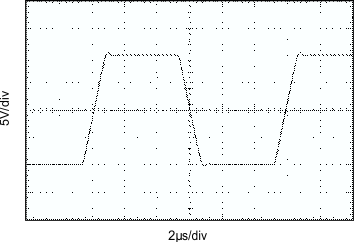
| Settling Time: 0.01% | VOUT = 10V Step | 2.5 | µs | |||||
| Overload Recovery | Output Overdriven 10% | 3 | µs | |||||
| POWER SUPPLY | ||||||||
| VS | Rated Voltage | ±18 | V | |||||
| Voltage Range | ±4.5 | ±18 | V | |||||
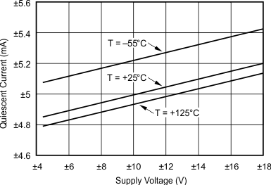
| IQ | Quiescent Current | IO = 0 | –5.5 | ±5.2 | 5.5 | mA | ||
| TEMPERATURE RANGE | ||||||||
| Specification Range | –40 | 85 | °C | |||||
| Operation Range | –55 | 125 | °C | |||||
| Storage Range | –55 | 125 | °C | |||||
| θJA | Thermal Resistance | 8-Pin DIP | 100 | °C/W | ||||
| SO-8 Surface mount | 150 | °C/W | ||||||
| SOL-16 Surface mount | 80 | °C/W | ||||||
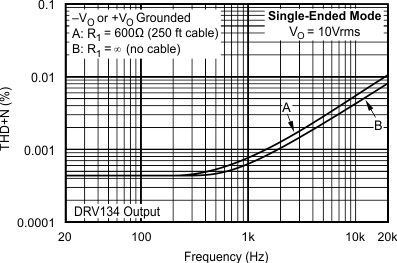
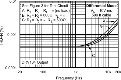
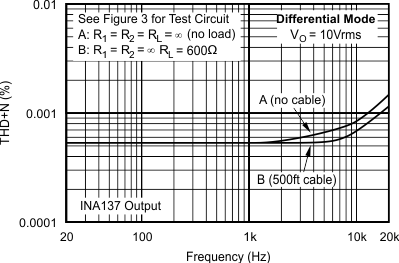
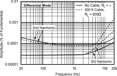
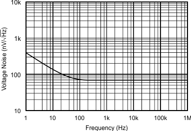
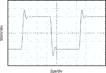
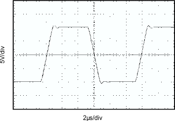
7.5 Typical Characteristics
At TA = 25°C, VS = ±18 V, RL = 600 Ω differential connected between +VO and –VO, unless otherwise noted.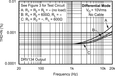
vs Frequency
vs Frequency
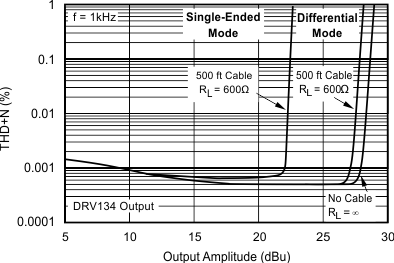
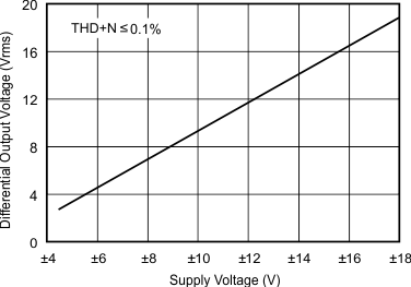
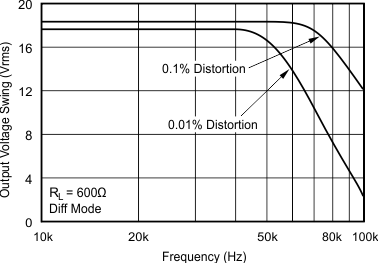
vs Output Amplitude
vs Frequency
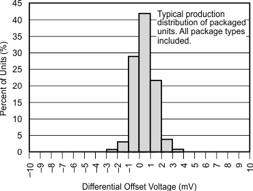
Production Distribution
| CL = 100 pF | ||
| CL = 100 pF | ||
vs Output Amplitude
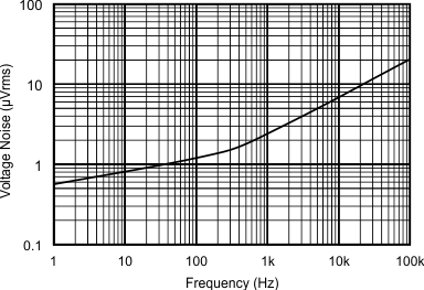
vs Noise Bandwidth
Production Distribution
| CL = 1000 pF | ||
| CL = 1000 pF | ||