SBOS094B January 1998 – December 2014 DRV134 , DRV135
PRODUCTION DATA.
- 1 Features
- 2 Applications
- 3 Description
- 4 Simplified Schematic
- 5 Revision History
- 6 Pin Configuration and Functions
- 7 Specifications
- 8 Detailed Description
- 9 Application and Implementation
- 10Power Supply Recommendations
- 11Layout
- 12Device and Documentation Support
- 13Mechanical, Packaging, and Orderable Information
Package Options
Mechanical Data (Package|Pins)
- D|8
Thermal pad, mechanical data (Package|Pins)
Orderable Information
11 Layout
11.1 Layout Guidelines
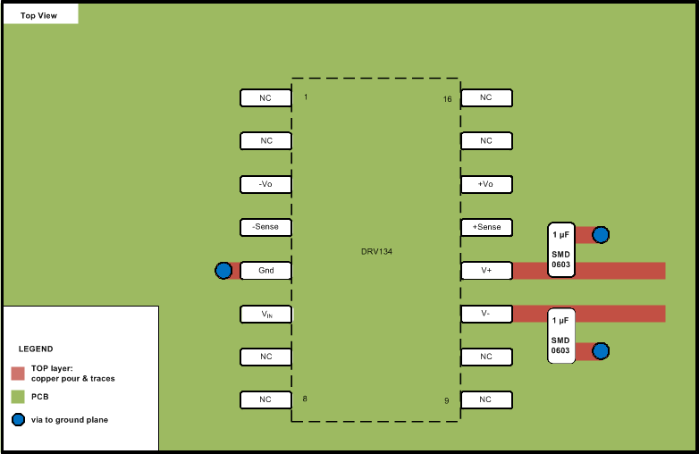
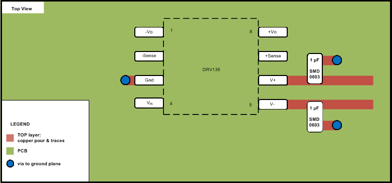
A driver/receiver balanced-pair (such as the DRV134 and INA137) rejects the voltage differences between the grounds at each end of the cable, which can be caused by ground currents, supply variations, etc. In addition to proper bypassing (as shown in Figure 32 and Figure 33), the suggestions below should be followed to achieve optimal OCMR and noise rejection.
- The DRV134 input should be driven by a low impedance source such as an op amp or buffer.
- As is the case for any single-ended system, the source’s common should be connected as close as possible to the DRV134’s ground. Any ground offset errors in the source will degrade system performance.
- Symmetry on the outputs should be maintained.
- Shielded twisted-pair cable is recommended for all applications. Physical balance in signal wiring should be maintained. Capacitive differences due to varying wire lengths may result in unequal noise pickup between the pair and degrade OCMR. Follow industry practices for proper system grounding of the cables.
11.2 Layout Examples
 Figure 32. DRV134 Layout Example
 Figure 33. DRV135 Layout Example
11.3 Thermal Performance
The DRV134 and DRV135 have robust output drive capability and excellent performance over temperature. In most applications there is no significant difference between the DIP, SOL-16, and SO-8 packages. However, for applications with extreme temperature and load conditions, the SOL-16 (DRV134UA) or DIP (DRV134PA) packages are recommended. Under these conditions, such as loads greater than 600 Ω or very long cables, performance may be degraded in the SO-8 (DRV135UA) package.