SLOS861C March   2015  – January 2023 DRV2700

PRODUCTION DATA  

  1. Features
  2. Applications
  3. Description
  4. Revision History
  5. Pin Configuration and Functions
  6. Specifications
    1. 6.1 Absolute Maximum Ratings
    2. 6.2 ESD Ratings
    3. 6.3 Recommended Operating Conditions
    4. 6.4 Thermal Information
    5. 6.5 Electrical Characteristics
    6. 6.6 Switching Characteristics
    7. 6.7 Typical characteristics
  7. Detailed Description
    1. 7.1 Overview
    2. 7.2 Functional Block Diagram
    3. 7.3 Feature Description
      1. 7.3.1 Boost Converter and Control Loop
      2. 7.3.2 High-Voltage Amplifier
      3. 7.3.3 Fast Start-Up (Enable Pin)
      4. 7.3.4 Gain Control
      5. 7.3.5 Adjustable Boost Voltage
      6. 7.3.6 Adjustable Boost Current-Limit
      7. 7.3.7 Internal Charge Pump
      8. 7.3.8 Thermal Shutdown
    4. 7.4 Device Functional Modes
      1. 7.4.1 Boost + Amplifier Mode
      2. 7.4.2 Flyback Mode
  8. Application and Implementation
    1. 8.1 Application Information
    2. 8.2 Typical Applications
      1. 8.2.1 AC-Coupled DAC Input Application
        1. 8.2.1.1 Design Requirements
        2. 8.2.1.2 Detailed Design Procedure
          1. 8.2.1.2.1  Piezo Load Selection
          2. 8.2.1.2.2  Programming The Boost Voltage
          3. 8.2.1.2.3  Inductor and Transformer Selection
          4. 8.2.1.2.4  Programing the Boost and Flyback Current-Limit
          5. 8.2.1.2.5  Boost Capacitor Selection
          6. 8.2.1.2.6  Pulldown FET and Resistors
          7. 8.2.1.2.7  Low-Voltage Operation
          8. 8.2.1.2.8  Current Consumption Calculation
          9. 8.2.1.2.9  Input Filter Considerations
          10. 8.2.1.2.10 Output Limiting Factors
          11. 8.2.1.2.11 Startup and Shutdown Sequencing
        3. 8.2.1.3 Application Curves
      2. 8.2.2 Filtered AC Coupled Single-Ended PWM Input Application
      3. 8.2.3 DC-Coupled DAC Input Application
      4. 8.2.4 DC-Coupled Reference Input Application
      5. 8.2.5 Flyback Circuit
    3. 8.3 System Example
  9. Power Supply Recommendations
  10. 10Layout
    1. 10.1 Layout Guidelines
      1. 10.1.1 Boost + Amplifier Configuration Layout Considerations
      2. 10.1.2 Flyback Configuration Layout Considerations
    2. 10.2 Layout Example
  11. 11Device and Documentation Support
    1. 11.1 Documentation Support
      1. 11.1.1 Related Documentation
    2. 11.2 Trademarks
  12. 12Mechanical, Packaging, and Orderable Information

Package Options

Refer to the PDF data sheet for device specific package drawings

Mechanical Data (Package|Pins)
  • RGP|20
Thermal pad, mechanical data (Package|Pins)
Orderable Information

Typical characteristics

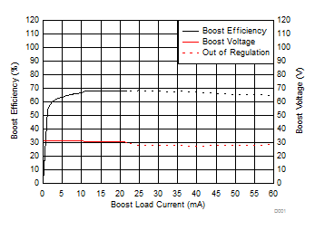
VDD = 3.6 V, R(REXT) = 7.5 kΩ, L = 4.7 µH, differential input, 100-nF DC blocking capacitors on IN±
GUID-A515A33C-CCBD-42B9-82C9-9392312DF9A6-low.gif
VDD = 3.6 VC(LOAD) = OpenVPVDD = 30 V
G = 28.8 dB
Figure 6-1 Load Current vs Boost Efficiency (%) and Voltage (V) at VPVDD = 30 V
GUID-8635C00D-D8BC-4CDA-98E7-081960CFCEE0-low.gif
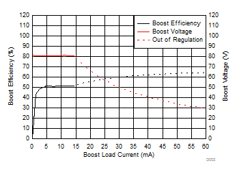
VDD = 3.6 VC(LOAD) = OpenVPVDD = 80 V
G = 38.4 dB
Figure 6-3 Load Current vs Boost Efficiency (%) and Voltage (V) at VPVDD = 80 V
GUID-EA42C4B8-6139-492D-A64B-483B9BEDB4CD-low.gif
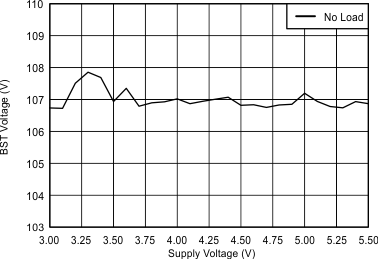
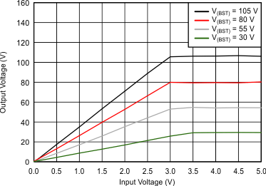
G = 40.7 dBC(LOAD) = OpenVPVDD = 105 V
Figure 6-5 Line Regulation at PVDD = 105 V
GUID-8696F6C7-FF0F-4919-89D8-7B437276AEE5-low.gif
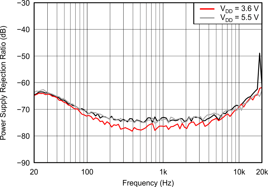
G = 40.7 dBC(LOAD) = OpenVPVDD = 105 V
Figure 6-7 AC PSRR at VPVDD = 105 V
GUID-AAAA284B-6A88-4F2A-9C01-CB7D5759D2B4-low.gif
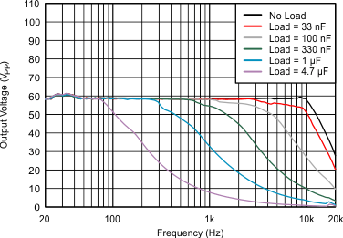
VDD = 3.6 VG = 28.8 dBVPVDD = 30 V
Figure 6-9 Gain Bandwidth at VPVDD = 30 V
GUID-B40613C4-883D-4068-91E6-E532CB231AE8-low.gif
VDD = 3.6 VG = 38.4 dBVPVDD = 80 V
Figure 6-11 Gain Bandwidth at VPVDD = 80 V
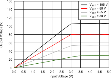
GUID-9C6050C1-6878-4890-9DB8-880FEEA7CC53-low.gif
VDD = 3.6 VG = 40.7 dBC(LOAD) = Open
Figure 6-13 Output Linearity
GUID-AC560349-106E-40B4-973A-86A35377F619-low.gif
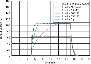
VDD = 3.6 VC(LOAD) = OpenVPVDD = 105 V
G = 40.7 dB
Figure 6-15 Output Slew Rate
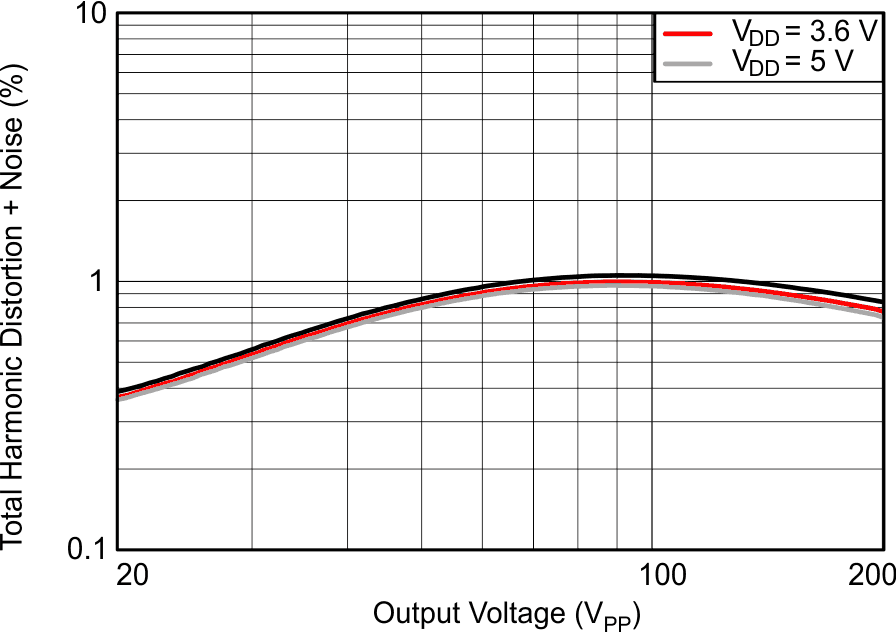
GUID-C821B2B0-DB1E-4D0A-A27F-E175E64D4085-low.gif
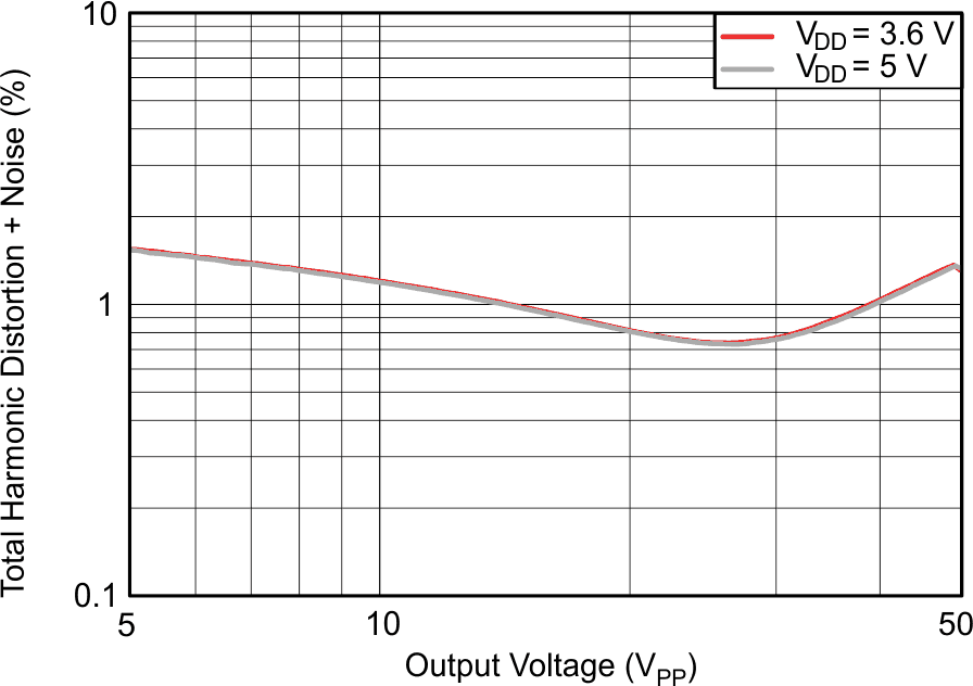
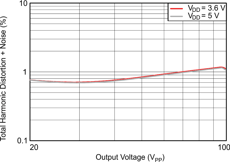
ƒ = 200 HzC(LOAD) = 47 nFVPVDD = 105 V
G = 40 dB
Figure 6-17 Total Harmonic Distortion + Noise vs Output Voltage
GUID-E8FD85B1-0C93-4204-BE5E-A1ED9C4503EF-low.gif
ƒ = 200 HzC(LOAD) = 680 nFVPVDD = 30 V
G = 28 dB
Figure 6-19 Total Harmonic Distortion + Noise vs Output Voltage
GUID-A7917EB0-3D50-417D-ABD8-2A38AFF28777-low.gif
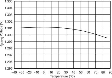
VDD = 3.6 VC(LOAD) = OpenVPVDD = 105 V
G = 40.7 dB
Figure 6-21 R(REXT) Voltage vs Temperature
GUID-9761C05D-588E-446B-A620-E25FCEDC85F8-low.gif
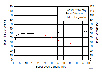
VDD = 3.6 VC(LOAD) = OpenVPVDD = 55 V
G = 34.8 dB
Figure 6-2 Load Current vs Boost Efficiency (%) and Voltage (V) at VPVDD = 55 V
GUID-655A00B8-B94E-440C-A817-2BCFFD40E49C-low.gif
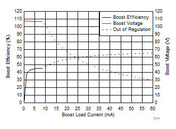
VDD = 3.6 VC(LOAD) = OpenVPVDD = 105 V
G = 40.7 dB
Figure 6-4 Load Current vs Boost Efficiency (%) and Voltage (V) at VPVDD = 105 V
GUID-FCD0A637-3173-41FC-9B4B-1E6FEF09A5C3-low.gif
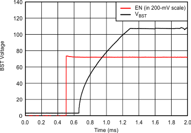
VDD = 3.6 VC(LOAD) = OpenVPVDD = 105 V
G = 40.7 dB
Figure 6-6 Boost Voltage Startup
GUID-A4592CEA-5B12-4D9B-B7B3-B241289031C8-low.gif
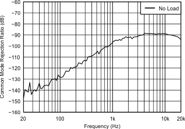
G = 40.7 dBC(LOAD) = OpenVPVDD = 105 V
Figure 6-8 AC CMRR at VPVDD = 105 V
GUID-BF7AFD26-F4C2-4531-9AB9-8120E159B89A-low.gif
VDD = 3.6 VG = 34.8 dBVPVDD = 55 V
Figure 6-10 Gain Bandwidth at VPVDD = 55 V
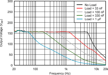
GUID-FEDF4126-7DC1-4A75-A6F9-95C4C0A1EB7F-low.gif
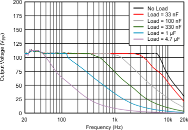
VDD = 3.6 VG = 40.7 dBVPVDD = 105 V
Figure 6-12 Gain Bandwidth at VPVDD = 105 V
GUID-393485E3-E0BA-4DC8-B443-A34A38E801AE-low.gif
VDD = 3.6 VC(LOAD) = Open
G = 28.8 dB at VPVDD = 30 VG = 34.8 dB at VPVDD = 55 V
G = 38.4 dB at VPVDD = 80 VG = 40.7 dB at VPVDD = 105 V
Figure 6-14 Output Linearity with Different Gains
GUID-209AF7FA-4F37-4688-A450-4F2567A2BA04-low.gif
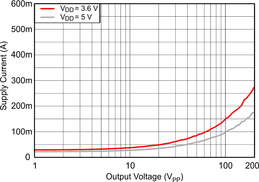
ƒ = 200 HzC(LOAD) = 47 nFVPVDD = 105 V
G = 40 dB
Figure 6-16 Supply Current vs Output Voltage
GUID-B80F1AFE-2B5D-4FC3-8956-FFE6892281D6-low.gif
ƒ = 200 HzC(LOAD) = 330 nFVPVDD = 55 V
G = 34 dB
Figure 6-18 Total Harmonic Distortion + Noise vs Output Voltage
GUID-B25BE074-CBDC-43B0-A4A8-77F3F06C9DD8-low.gif
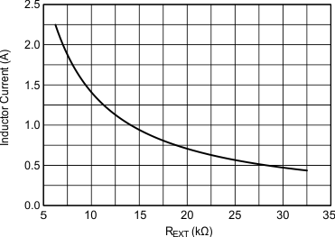
Figure 6-20 Inductor Current vs R(REXT)