6 Specifications
6.1 Absolute Maximum Ratings
over operating free-air temperature range (unless otherwise noted) (1)
|
MIN |
MAX |
UNIT |
| Power supply voltage |
VCC |
–22(2) |
40 |
V |
| Voltage ramp rate (VCC), VCC < 5 V |
Unlimited |
V/µs |
| Voltage ramp rate (VCC), VCC > 5 V |
0 |
2 |
| Output pin voltage |
–0.5 |
40 |
V |
| Output pin reverse current during reverse supply condition |
0 |
100 |
mA |
| Magnetic flux density, BMAX |
Unlimited |
|
| Operating junction temperature, TJ |
Q, see Figure 24 |
–40 |
150 |
°C |
| E, see Figure 24 |
–40 |
17 |
| Storage temperature, Tstg |
–65 |
150 |
°C |
(1) Stresses beyond those listed under Absolute Maximum Ratings may cause permanent damage to the device. These are stress ratings only, which do not imply functional operation of the device at these or any other conditions beyond those indicated under Recommended Operating Conditions. Exposure to absolute-maximum-rated conditions for extended periods may affect device reliability.
(2) Ensured by design. Only tested to –20 V.
6.2 ESD Ratings
|
VALUE |
UNIT |
| V(ESD) |
Electrostatic discharge |
Human-body model (HBM), per AEC Q100-002(1) |
±2500 |
V |
| Charged-device model (CDM), per AEC Q100-011 |
±500 |
(1) AEC Q100-002 indicates that HBM stressing shall be in accordance with the ANSI/ESDA/JEDEC JS-001 specification.
6.3 Recommended Operating Conditions
over operating free-air temperature range (unless otherwise noted)
|
MIN |
MAX |
UNIT |
| VCC |
Power supply voltage |
2.7 |
38 |
V |
| VO |
Output pin voltage (OUT) |
0 |
38 |
V |
| ISINK |
Output pin current sink (OUT)(1) |
0 |
30 |
mA |
| TA |
Operating ambient temperature |
Q, see Figure 24 |
–40 |
125 |
°C |
| E, see Figure 24 |
–40 |
150 |
(1) Power dissipation and thermal limits must be observed
6.4 Thermal Information
| THERMAL METRIC(1) |
DRV5033-Q1 |
UNIT |
| DBZ (SOT-23) |
LPG (TO-92) |
| 3 PINS |
3 PINS |
| RθJA |
Junction-to-ambient thermal resistance |
333.2 |
180 |
°C/W |
| RθJC(top) |
Junction-to-case (top) thermal resistance |
99.9 |
98.6 |
°C/W |
| RθJB |
Junction-to-board thermal resistance |
66.9 |
154.9 |
°C/W |
| ψJT |
Junction-to-top characterization parameter |
4.9 |
40 |
°C/W |
| ψJB |
Junction-to-board characterization parameter |
65.2 |
154.9 |
°C/W |
(1) For more information about traditional and new thermal metrics, see the
Semiconductor and IC Package Thermal Metrics application report,
SPRA953.
6.5 Electrical Characteristics
over operating free-air temperature range (unless otherwise noted)
| PARAMETER |
TEST CONDITIONS |
MIN |
TYP |
MAX |
UNIT |
| POWER SUPPLIES (VCC) |
|
|
|
|
| VCC |
VCC operating voltage |
|
2.7 |
|
38 |
V |
| ICC |
Operating supply current |
VCC = 2.7 to 38 V, TA = 25°C |
|
2.7 |
|
mA |
| VCC = 2.7 to 38 V, TA = TA, MAX(1) |
|
3 |
3.6 |
| ton |
Power-on time |
AJ version |
|
35 |
50 |
µs |
| FA version |
|
35 |
70 |
| OPEN DRAIN OUTPUT (OUT) |
| rDS(on) |
FET on-resistance |
VCC = 3.3 V, IO = 10 mA, TA = 25°C |
|
22 |
|
Ω |
| VCC = 3.3 V, IO = 10 mA, TA = 125°C |
|
36 |
50 |
| Ilkg(off) |
Off-state leakage current |
Output Hi-Z |
|
|
1 |
µA |
| PROTECTION CIRCUITS |
| VCCR |
Reverse supply voltage |
|
–22 |
|
|
V |
| IOCP |
Overcurrent protection level |
OUT shorted VCC |
15 |
30 |
45 |
mA |
(1) T
A, MAX is 125°C for Q Grade 1 devices and 150°C for E Grade 0 devices (see
Figure 24)
6.6 Switching Characteristics
over operating free-air temperature range (unless otherwise noted)
| PARAMETER |
TEST CONDITIONS |
MIN |
TYP |
MAX |
UNIT |
| OPEN DRAIN OUTPUT (OUT) |
|
|
|
|
| td |
Output delay time |
B = BRP – 10 mT to BOP + 10 mT in 1 µs |
|
13 |
25 |
µs |
| tr |
Output rise time (10% to 90%) |
R1 = 1 kΩ, CO = 50 pF, VCC = 3.3 V |
|
200 |
|
ns |
| tf |
Output fall time (90% to 10%) |
R1 = 1 kΩ, CO = 50 pF, VCC = 3.3 V |
|
31 |
|
ns |
6.7 Magnetic Characteristics
over operating free-air temperature range (unless otherwise noted)
| PARAMETER |
TEST CONDITIONS |
MIN |
TYP |
MAX |
UNIT(1) |
| ƒBW |
Bandwidth(2) |
|
20 |
30 |
|
kHz |
| DRV5033FA: ±3.5 / ±2 mT |
|
|
|
|
| BOP |
Operate point; see Figure 12 |
|
±1.8 |
±3.5 |
±6.8 |
mT |
| BRP |
Release point; see Figure 12 |
±0.5 |
±2 |
±4.2 |
mT |
| Bhys |
Hysteresis; Bhys = (BOP – BRP)(3) |
|
±1.5 |
|
mT |
| BO |
Magnetic offset; BO = (BOP + BRP) / 2 |
|
±2.8 |
|
mT |
| DRV5033AJ: ±6.9 / ±3.5 mT |
|
|
|
|
| BOP |
Operate point; see Figure 12 |
|
±3 |
±6.9 |
±12 |
mT |
| BRP |
Release point; see Figure 12 |
±1 |
±3.5 |
±5 |
mT |
| Bhys |
Hysteresis; Bhys = (BOP – BRP)(3) |
|
3.4 |
|
mT |
| BO |
Magnetic offset; BO = (BOP + BRP) / 2 |
|
5.2 |
|
mT |
(1) 1 mT = 10 Gauss
(2) Bandwidth describes the fastest changing magnetic field that can be detected and translated to the output.
(3) |BOP| is always greater than |BRP|.
6.8 Typical Characteristics
TA > 125°C data is valid for Grade 0 devices only (E, see Figure 24)
 Figure 1. ICC vs VCC
 Figure 3. DRV5033-Q1AJ, BOP vs VCC
 Figure 5. DRV5033-Q1AJ, BRP vs VCC
 Figure 7. DRV5033-Q1AJ, Hysteresis vs VCC
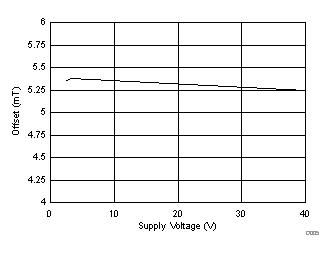
 Figure 9. DRV5033-Q1AJ, Offset vs VCC
 Figure 2. ICC vs Temperature
 Figure 4. DRV5033-Q1AJ, BOP vs Temperature
 Figure 6. DRV5033-Q1AJ, BRP vs Temperature
 Figure 8. DRV5033-Q1AJ, Hysteresis vs Temperature
 Figure 10. DRV5033-Q1AJ, Offset vs Temperature


