SBAS639D October 2017 – June 2024 DRV5055-Q1
PRODUCTION DATA
- 1
- 1 Features
- 2 Applications
- 3 Description
- 4 Pin Configuration and Functions
- 5 Specifications
- 6 Detailed Description
- 7 Application and Implementation
- 8 Device and Documentation Support
- 9 Revision History
- 10Mechanical, Packaging, and Orderable Information
Package Options
Mechanical Data (Package|Pins)
Thermal pad, mechanical data (Package|Pins)
Orderable Information
3 Description
The DRV5055-Q1 is a linear Hall effect sensor that responds proportionally to magnetic flux density. The device can be used for accurate position sensing in a wide range of applications.
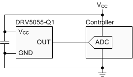
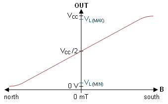
The device operates from 3.3V or 5V power supplies. When no magnetic field is present, the analog output drives half of VCC. The output changes linearly with the applied magnetic flux density, and various sensitivity options enable maximal output voltage swing based on the required sensing range. North and south magnetic poles produce unique voltages.
Magnetic flux perpendicular to the top of the package is sensed, and the two package options provide different sensing directions.
The device uses a ratiometric architecture that can eliminate error from VCC tolerance when the external analog-to-digital converter (ADC) uses the same VCC for its reference. Additionally, the device features magnet temperature compensation to counteract how magnets drift for linear performance across a wide –40°C to +150°C temperature range.
| PART NUMBER | PACKAGE(1) | PACKAGE SIZE(2) |
|---|---|---|
| DRV5055-Q1 | DBZ (SOT-23, 3) | 2.92mm × 2.37mm |
| LPG (TO-92, 3) | 4mm × 1.52mm |
 Typical
Schematic
 Magnetic Response (A1, A2, A3, A4, Z2 Versions)