SBAS639D October   2017  – June 2024 DRV5055-Q1

PRODUCTION DATA  

  1.   1
  2. Features
  3. Applications
  4. Description
  5. Pin Configuration and Functions
  6. Specifications
    1. 5.1 Absolute Maximum Ratings
    2. 5.2 ESD Ratings
    3. 5.3 Recommended Operating Conditions
    4. 5.4 Thermal Information
    5. 5.5 Electrical Characteristics
    6. 5.6 Magnetic Characteristics
    7. 5.7 Typical Characteristics
  7. Detailed Description
    1. 6.1 Overview
    2. 6.2 Functional Block Diagram
    3. 6.3 Feature Description
      1. 6.3.1 Magnetic Flux Direction
      2. 6.3.2 Magnetic Response
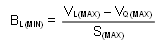
      3. 6.3.3 Sensitivity Linearity
      4. 6.3.4 Ratiometric Architecture
      5. 6.3.5 Operating VCC Ranges
      6. 6.3.6 Sensitivity Temperature Compensation for Magnets
      7. 6.3.7 Power-On Time
      8. 6.3.8 Hall Element Location
    4. 6.4 Device Functional Modes
  8. Application and Implementation
    1. 7.1 Application Information
      1. 7.1.1 Selecting the Sensitivity Option
      2. 7.1.2 Temperature Compensation for Magnets
      3. 7.1.3 Adding a Low-Pass Filter
      4. 7.1.4 Designing for Wire Break Detection
    2. 7.2 Typical Application
      1. 7.2.1 Design Requirements
      2. 7.2.2 Detailed Design Procedure
      3. 7.2.3 Application Curve
    3. 7.3 Best Design Practices
    4. 7.4 Power Supply Recommendations
    5. 7.5 Layout
      1. 7.5.1 Layout Guidelines
      2. 7.5.2 Layout Examples
  9. Device and Documentation Support
    1. 8.1 Documentation Support
      1. 8.1.1 Related Documentation
    2. 8.2 Receiving Notification of Documentation Updates
    3. 8.3 Support Resources
    4. 8.4 Trademarks
    5. 8.5 Electrostatic Discharge Caution
    6. 8.6 Glossary
  10. Revision History
  11. 10Mechanical, Packaging, and Orderable Information

Package Options

Mechanical Data (Package|Pins)
Thermal pad, mechanical data (Package|Pins)
Orderable Information

Sensitivity Linearity

The device produces a linear response when the output voltage is within the specified VL range. Outside this range, sensitivity is reduced and nonlinear. Figure 6-3 graphs the magnetic response.

DRV5055-Q1 Magnetic Response Figure 6-3 Magnetic Response

Equation 2 calculates parameter BL, the minimum linear sensing range at 25°C taking into account the maximum quiescent voltage and sensitivity tolerances.

Equation 2. DRV5055-Q1

The parameter SLE defines linearity error as the difference in sensitivity between any two positive B values, and any two negative B values, while the output is within the VL range.

The parameter SSE defines symmetry error as the difference in sensitivity between any positive B value and the negative B value of the same magnitude, while the output voltage is within the VL range.