SLVSFY8B February   2020  – August 2021 DRV8210

PRODUCTION DATA  

  1. Features
  2. Applications
  3. Description
  4. Revision History
  5. Device Comparison
  6. Pin Configuration and Functions
  7. Specifications
    1. 7.1 Absolute Maximum Ratings
    2. 7.2 ESD Ratings
    3. 7.3 Recommended Operating Conditions
    4. 7.4 Thermal Information
    5. 7.5 Electrical Characteristics
    6. 7.6 Typical Characteristics DSG Package
    7. 7.7 Typical Characteristics DRL Package
  8. Detailed Description
    1. 8.1 Overview
    2. 8.2 Functional Block Diagram
    3. 8.3 Feature Description
      1. 8.3.1 External Components
      2. 8.3.2 Control Modes
        1. 8.3.2.1 PWM Control Mode (DSG: MODE = 0 and DRL)
        2. 8.3.2.2 PH/EN Control Mode (DSG: MODE = 1)
        3. 8.3.2.3 Half-Bridge Control Mode (DSG: MODE = Hi-Z)
      3. 8.3.3 Protection Circuits
        1. 8.3.3.1 Supply Undervoltage Lockout (UVLO)
        2. 8.3.3.2 OUTx Overcurrent Protection (OCP)
        3. 8.3.3.3 Thermal Shutdown (TSD)
      4. 8.3.4 Pin Diagrams
        1. 8.3.4.1 Logic-Level Inputs
        2. 8.3.4.2 Tri-Level Input
    4. 8.4 Device Functional Modes
      1. 8.4.1 Active Mode
      2. 8.4.2 Low-Power Sleep Mode
      3. 8.4.3 Fault Mode
  9. Application and Implementation
    1. 9.1 Application Information
    2. 9.2 Typical Application
      1. 9.2.1 Full-Bridge Driving
        1. 9.2.1.1 Design Requirements
        2. 9.2.1.2 Detailed Design Procedure
          1. 9.2.1.2.1 Supply Voltage
          2. 9.2.1.2.2 Control Interface
          3. 9.2.1.2.3 Low-Power Operation
        3. 9.2.1.3 Application Curves
      2. 9.2.2 Half-Bridge Driving
        1. 9.2.2.1 Design Requirements
        2. 9.2.2.2 Detailed Design Procedure
          1. 9.2.2.2.1 Supply Voltage
          2. 9.2.2.2.2 Control Interface
          3. 9.2.2.2.3 Low-Power Operation
        3. 9.2.2.3 Application Curves
      3. 9.2.3 Dual-Coil Relay Driving
        1. 9.2.3.1 Design Requirements
        2. 9.2.3.2 Detailed Design Procedure
          1. 9.2.3.2.1 Supply Voltage
          2. 9.2.3.2.2 Control Interface
          3. 9.2.3.2.3 Low-Power Operation
        3. 9.2.3.3 Application Curves
      4. 9.2.4 Current Sense
        1. 9.2.4.1 Design Requirements
        2. 9.2.4.2 Detailed Design Procedure
          1. 9.2.4.2.1 Shunt Resistor Sizing
          2. 9.2.4.2.2 RC Filter
    3. 9.3 Current Capability and Thermal Performance
      1. 9.3.1 Power Dissipation and Output Current Capability
      2. 9.3.2 Thermal Performance
        1. 9.3.2.1 Steady-State Thermal Performance
        2. 9.3.2.2 Transient Thermal Performance
  10. 10Power Supply Recommendations
    1. 10.1 Bulk Capacitance
  11. 11Layout
    1. 11.1 Layout Guidelines
    2. 11.2 Layout Example
  12. 12Device and Documentation Support
    1. 12.1 Documentation Support
      1. 12.1.1 Related Documentation
    2. 12.2 Receiving Notification of Documentation Updates
    3. 12.3 Support Resources
    4. 12.4 Trademarks
    5. 12.5 Electrostatic Discharge Caution
    6. 12.6 Glossary
  13. 13Mechanical, Packaging, and Orderable Information

Package Options

Mechanical Data (Package|Pins)
Thermal pad, mechanical data (Package|Pins)
Orderable Information

Control Modes

The DRV8210 provides three modes to support different control schemes with the PH/IN1 and EN/IN2 pins. The MODE pin selects the control interface mode by setting it either logic low, logic high, or Hi-Z as shown in Table 8-2. The MODE pin does not latch its state, so it may be changed during operation.

The DRL package variant only supports the PWM interface (see Table 8-3).

Table 8-2 MODE pin functions for DSG variant
MODE STATE CONTROL MODE
MODE = Logic Low PWM
MODE = Logic High PH/EN
MODE = Hi-Z Half-Bridge

The inputs can accept DC or pulse-width modulated (PWM) voltage signals with duty cycles from 0% to 100%. By default, the INx, PH/IN1, and EN/IN2 pins have internal pulldown resistors to ensure the outputs are Hi-Z if no inputs are present (the only exception is half-bridge mode, where OUTx = L if INx is floating).

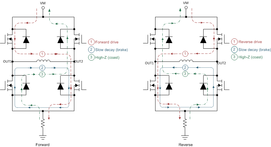
The following sections show the truth tables for each control mode. Additionally, the DRV8210 automatically handles the dead-time generation when switching between the high-side and low-side MOSFET of a half-bridge. Figure 8-3 describes the naming and configuration for the various H-bridge states described in the following sections.
GUID-FF5A2ACA-6802-4E19-BB8D-7DBD46CAD9A6-low.gif Figure 8-3 H-bridge states