SLVSHO5 April 2024 DRV8215
PRODUCTION DATA
- 1
- 1 Features
- 2 Applications
- 3 Description
- 4 Device Comparison
- 5 Pin Configuration and Functions
- 6 Specifications
-
7 Detailed Description
- 7.1 Overview
- 7.2 Functional Block Diagram
- 7.3
Feature Description
- 7.3.1 External Components
- 7.3.2 Summary of Features
- 7.3.3 Bridge Control
- 7.3.4 Current Sense and Regulation (IPROPI)
- 7.3.5 Stall Detection
- 7.3.6 Motor Voltage and Speed Regulation
- 7.3.7 Protection Circuits
- 7.4 Device Functional Modes
- 7.5 Programming
- 8 Register Map
- 9 Application and Implementation
- 10Device and Documentation Support
- 11Revision History
- 12Mechanical, Packaging, and Orderable Information
Package Options
Mechanical Data (Package|Pins)
- RTE|16
Thermal pad, mechanical data (Package|Pins)
- RTE|16
Orderable Information
7.3.4.1 Current Sensing and Current Mirror Gain Selection
The IPROPI pin outputs an analog current proportional to the current flowing through the low-side power MOSFETs in the H-bridge and scaled by the current mirror gain (AIPROPI). The IPROPI output current can be calculated by the following equation. The ILSx in the equation is only valid when the current flows from drain to source in the low-side MOSFET. If current flows from source to drain or through the body diode, the value of ILSx for that channel is zero. For instance, if the bridge is in the brake, slow-decay state, then the current out of IPROPI is only proportional to the current in one of the low-side MOSFETs.
The AERR parameter in the Electrical Characteristics table is the error associated with the AIPROPI gain. It indicates the combined effect of offset error added to the IOUT current and gain error.
The current mirror gain AIPROPI depends on the CS_GAIN_SEL bit setting, as shown in the table below -
| CS_GAIN_SEL | AIPROPI | Recommended Current Range | Low-side FET RDS(ON) | Minimum OCP Limit |
|---|---|---|---|---|
000b | 244 μA/A | 350 mA to 2A | 120 mΩ | 4 A |
010b | 1156 μA/A | 60 mA to 350 mA | 440 mΩ | 800 mA |
110b | 5320 μA/A | 10 mA to 60 mA | 2040 mΩ | 160 mA |
CS_GAIN_SEL bits therefore allows optimizing the design for various applications by reducing OCP limit and increasing current mirror gain at lower motor currents.
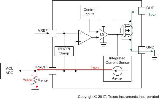
The motor current is measured by an internal current mirror architecture on the low-side FETs which removes the need for an external power sense resistor as shown below. The current mirror architecture senses motor winding current in both the drive and brake low-side slow-decay periods, therefore allowing continuous current monitoring in typical bidirectional brushed DC motor applications. In coast mode, the current is freewheeling and cannot be sensed because it flows from source to drain. However, the current can be sampled by briefly reenabling the driver in either drive or slow-decay modes and measuring the current before switching back to coast mode again.
Table 7-7 lists the overall CS_GAIN_SEL settings with the maximum current values.
| Bit | Maximum Current Value | AIPROPI |
|---|---|---|
| 000b | 4 A | 244 μA/A |
| 001b | 2 A | 244 μA/A |
| 010b | 1 A | 1156 μA/A |
| 011b | 0.5 A | 1156 μA/A |
| 1X0b | 0.25 A | 5320 μA/A |
| 1X1b | 0.125 A | 5320 μA/A |
 Figure 7-4 Integrated Current Sensing
The IPROPI pin should be connected to an external resistor (RIPROPI) to ground in order to generate a proportional voltage (VIPROPI) on the IPROPI pin with the IIPROPI analog current output. This allows for the load current to be measured as the voltage drop across the RIPROPI resistor with a standard analog to digital converter (ADC). The RIPROPI resistor can be sized based on the expected load current in the application so that the full range of the controller ADC is utilized.
Additionally, the DRV8215 implements an internal IPROPI voltage clamp circuit to limit VIPROPI with respect to VVREF on the VREF pin and protect the external ADC in case of output overcurrent or unexpected high current events. TI recommends designing for at least 1.25 V of headroom between VVM and the maximum VIPROPI voltage to be measured by the ADC, VIPROPI_MAX. This ensures good accuracy across the range of VIPROPI voltages measured by the ADC. For instance, if VVM is 4.55 V to 11 V, VIPROPI_MAX can be as high as 3.3 V. However, if VVM is 3.3 V, then VIPROPI will have good accuracy up to 2.05 V.
The corresponding IPROPI voltage to the output current can be calculated as shown below -
The IPROPI output bandwidth is limited by the sense delay time (tDELAY) of the internal current sensing circuit. This time is the delay from the low-side MOSFET enable command (from the INx pins) to the IPROPI output being ready.
If the device is alternating between drive and slow-decay (brake) in an H-bridge PWM pattern then the low-side MOSFET sensing the current is continuously on and the sense delay time has no impact to the IPROPI output. If a command on the INx pins disables the low-side MOSFETs (according to the truth tables), the IPROPI output will disable with the input logic signal. Although the low-side MOSFETs may still conduct current as they disable according to the device slew rate (specified in the Electrical Characteristics table by tRISE time), IPROPI will not represent the current in the low-side MOSFETs during this turnoff time.