SLVSFV5B July 2023 – October 2024 DRV8262
PRODUCTION DATA
- 1
- 1 Features
- 2 Applications
- 3 Description
- 4 Pin Configuration and Functions
- 5 Specifications
-
6 Detailed Description
- 6.1 Overview
- 6.2 Functional Block Diagram
- 6.3 Feature Description
- 6.4 Device Operational Modes
- 6.5 Current Sensing and Regulation
- 6.6 Charge Pump
- 6.7 Linear Voltage Regulator
- 6.8 VCC Voltage Supply
- 6.9 Logic Level, Tri-Level and Quad-Level Pin Diagrams
- 6.10 Protection Circuits
- 6.11 Device Functional Modes
- 7 Application and Implementation
- 8 Package Thermal Considerations
- 9 Device and Documentation Support
- 10Revision History
- 11Mechanical, Packaging, and Orderable Information
Package Options
Mechanical Data (Package|Pins)
Thermal pad, mechanical data (Package|Pins)
- DDW|44
Orderable Information
6.5.2 Current Regulation
The current chopping threshold (ITRIP) is set through a combination of the VREF voltage (VVREF) and IPROPI output resistor (RIPROPI). This is done by comparing the voltage drop across the external RIPROPI resistor to VVREF with an internal comparator.
For example, in the dual H-bridge mode, to set ITRIP at 5 A with VVREF at 3.3V, RIPROPI has to be -
RIPROPI = VVREF / (ITRIP x AIPROPI ) = 3.3 / (5 x 212 x 10-6) = 3.09kΩ
In the single H-bridge mode, connect the two IPROPI pins. In the dual H-bridge mode, there are two VREF pins, which allows setting separate current chopping thresholds for each brushed-DC motor.
The internal current regulation can be disabled by tying IPROPI to GND and setting the VREF pin voltage greater than GND (if current feedback is not required). If current feedback is required and current regulation is not required, set VVREF and RIPROPI such that VIPROPI never reaches the VVREF threshold.
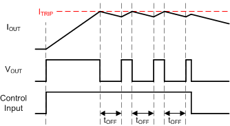
 Figure 6-5 Current Regulation
The current through the motor windings is regulated by an adjustable off-time PWM current regulation circuit. During PWM current chopping, the H-bridge is enabled to drive through the motor winding until the PWM current chopping threshold is reached.
When the ITRIP current has been reached, for single BDC or dual BDC applications, with the DECAY pin grounded, the device enforces slow current decay by enabling both the high-side FETs for a time of tOFF, programmed by the TOFF pin.
When the tOFF time has elapsed and the current level falls below the current regulation (ITRIP) level, the output is re-enabled according to the inputs. If, after the tOFF time has elapsed, the current is still higher than the ITRIP level, the device enforces another tOFF time period of the same duration. This "double tOFF" time continues until the current is less than ITRIP at the end of tOFF time.
In current regulation, the inputs can be toggled to drive the load in the opposite direction to decay the current faster. For example, if the load was in forward drive before entering the current regulation it can only go into reverse drive when the driver enforces current regulation.
For single or dual-BDC applications, the DECAY pin should be kept grounded for high-side slow decay during tOFF. For stepper applications, DECAY pin voltage should be according to the desired decay mode. The decay mode is selected by the DECAY pin as shown in Table 6-7.
| DECAY | DECAY MODE |
|---|---|
0 | Slow decay (brake or high-side re-circulation) |
| 1 | Smart tune dynamic decay |
| Hi-Z | Mixed decay: 30% fast |
If the state of the INx control pin inputs changes during the tOFF time, the remainder of the tOFF time is ignored, and the outputs will again follow the inputs. This is shown in Figure 6-6.
 Figure 6-6 Current Regulation
As shown in Table 6-8, the TOFF pin configures the PWM OFF time. The OFF time settings can be changed on the fly.
| TOFF | OFF-TIME (tOFF) |
|---|---|
| 0 | 7µs |
| 1 | 16µs |
| Hi-Z | 24µs |
| 330 kΩ to GND | 32µs |