SLOSE51A June 2020 – December 2020 DRV8428E
ADVANCE INFORMATION
- 1 Features
- 2 Applications
- 3 Description
- 4 Revision History
- 5 Pin Configuration and Functions
- 6 Specifications
- 7 Detailed Description
- 8 Application and Implementation
- 9 Power Supply Recommendations
- 10Layout
- 11Device and Documentation Support
- 12Mechanical, Packaging, and Orderable Information
Package Options
Mechanical Data (Package|Pins)
Thermal pad, mechanical data (Package|Pins)
Orderable Information
7.3.3 Current Regulation, Off-time and Decay Modes
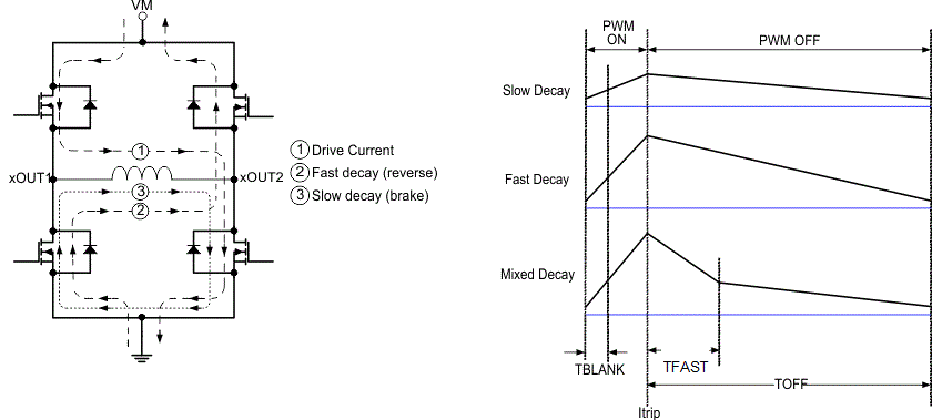
During PWM current chopping, the H-bridge is enabled to drive through the motor winding until the PWM current chopping threshold is reached. This is shown in Figure 7-5, Item 1.
The current through the motor windings is regulated by an adjustable, off-time PWM current-regulation circuit. When an H-bridge is enabled, current rises through the winding at a rate dependent on the DC voltage, inductance of the winding, and the magnitude of the back EMF present. When the current hits the current regulation threshold, the bridge enters a decay mode for a period of time determined by the seven-level DECAY/TOFF pin setting to decrease the current. After the off-time expires, the bridge is re-enabled, starting another PWM cycle.
Once the chopping current threshold is reached, the H-bridge can operate in two different states, fast decay or slow decay. In fast decay mode, once the PWM chopping current level has been reached, the H-bridge reverses state to allow winding current to flow in a reverse direction. The opposite FETs are turned on; as the winding current approaches zero, the bridge is disabled to prevent any reverse current flow. Fast decay mode is shown in Figure 7-5, item 2. In slow decay mode, winding current is re-circulated by enabling both of the low-side FETs in the bridge. This is shown in Figure 7-5, Item 3.
The PWM chopping current is set by a comparator which monitors the voltage across the current sense MOSFETs in parallel with the low-side power MOSFETs. To generate the reference voltage for the current chopping comparator, the VREFx input is attenuated by a factor of Kv.
The chopping current (IFS) can be calculated as IFS (A) = VREFx (V) / KV (V/A) = VREFx (V) / 3 (V/A).
 Figure 7-5 Decay Modes
The decay mode and off time for each bridge is selected by setting the seven-level DECAY/TOFF pin as shown in Table 7-4.
| DECAY/TOFF | DECAY MODE | OFF TIME |
|---|---|---|
| 0 | Smart tune Ripple Control | - |
| 14.7kΩ to GND | Mixed 30% Decay | 7µs |
| 44.2kΩ to GND | 16µs | |
| 100kΩ to GND | 32µs | |
| 249kΩ to GND | Smart tune Dynamic Decay | 7µs |
| Hi-Z | 16µs | |
| DVDD | 32µs |