SLOSE79B August 2022 – October 2023 DRV8462
PRODUCTION DATA
- 1
- 1 Features
- 2 Applications
- 3 Description
- 4 Revision History
- 5 Pin Configuration and Functions
- 6 Specifications
-
7 Detailed Description
- 7.1 Overview
- 7.2 Functional Block Diagram
- 7.3
Feature Description
- 7.3.1 Interface of Operation
- 7.3.2 Stepper Motor Driver Current Ratings
- 7.3.3 PWM Motor Drivers
- 7.3.4 Microstepping Indexer
- 7.3.5 Indexer Output
- 7.3.6 Automatic Microstepping Mode
- 7.3.7 Custom Microstepping Table
- 7.3.8 Current Regulation
- 7.3.9 Internal Reference Voltage
- 7.3.10 Standstill Power Saving Mode
- 7.3.11 Current Regulation Decay Modes
- 7.3.12 Current Sensing with External Resistor
- 7.3.13 Silent step decay mode
- 7.3.14 Auto-torque Dynamic Current Adjustment
- 7.3.15 Charge Pump
- 7.3.16 Linear Voltage Regulator
- 7.3.17 VCC Voltage Supply
- 7.3.18 Logic Level, Tri-Level and Quad-Level Pin Diagrams
- 7.3.19 Spread spectrum
- 7.3.20
Protection Circuits
- 7.3.20.1 VM Undervoltage Lockout
- 7.3.20.2 VCP Undervoltage Lockout (CPUV)
- 7.3.20.3 Logic Supply Power on Reset (POR)
- 7.3.20.4 Overcurrent Protection (OCP)
- 7.3.20.5 Stall Detection
- 7.3.20.6 Open-Load Detection (OL)
- 7.3.20.7 Overtemperature Warning (OTW)
- 7.3.20.8 Thermal Shutdown (OTSD)
- 7.3.20.9 Supply voltage sensing
- 7.3.20.10 nFAULT Output
- 7.3.20.11 Fault Condition Summary
- 7.3.21 Device Functional Modes
- 7.4 Programming
- 7.5
Register Maps
- 7.5.1 Status Registers
- 7.5.2
Control Registers
- 7.5.2.1 CTRL1 (address = 0x04) [Default = 0Fh]
- 7.5.2.2 CTRL2 (address = 0x05) [Default = 06h]
- 7.5.2.3 CTRL3 (address = 0x06) [Default = 38h]
- 7.5.2.4 CTRL4 (address = 0x07) [Default = 49h]
- 7.5.2.5 CTRL5 (address = 0x08) [Default = 03h]
- 7.5.2.6 CTRL6 (address = 0x09) [Default = 20h]
- 7.5.2.7 CTRL7 (address = 0x0A) [Default = FFh]
- 7.5.2.8 CTRL8 (address = 0x0B) [Default = 0Fh]
- 7.5.2.9 CTRL9 (address = 0x0C) [Default = 10h]
- 7.5.2.10 CTRL10 (address = 0x0D) [Default = 80h]
- 7.5.2.11 CTRL11 (address = 0x0E) [Default = FFh]
- 7.5.2.12 CTRL12 (address = 0x0F) [Default = 20h]
- 7.5.2.13 CTRL13 (address = 0x10) [Default = 10h]
- 7.5.2.14 CTRL14 (address = 0x3C) [Default = 58h]
- 7.5.3 Indexer Registers
- 7.5.4
Custom Microstepping Registers
- 7.5.4.1 CUSTOM_CTRL1 (address = 0x16) [Default = 00h]
- 7.5.4.2 CUSTOM_CTRL2 (address = 0x17) [Default = 00h]
- 7.5.4.3 CUSTOM_CTRL3 (address = 0x18) [Default = 00h]
- 7.5.4.4 CUSTOM_CTRL4 (address = 0x19) [Default = 00h]
- 7.5.4.5 CUSTOM_CTRL5 (address = 0x1A) [Default = 00h]
- 7.5.4.6 CUSTOM_CTRL6 (address = 0x1B) [Default = 00h]
- 7.5.4.7 CUSTOM_CTRL7 (address = 0x1C) [Default = 00h]
- 7.5.4.8 CUSTOM_CTRL8 (address = 0x1D) [Default = 00h]
- 7.5.4.9 CUSTOM_CTRL9 (address = 0x1E) [Default = 00h]
- 7.5.5
Auto torque Registers
- 7.5.5.1 ATQ_CTRL1 (address = 0x1F) [Default = 00h]
- 7.5.5.2 ATQ_CTRL2 (address = 0x20) [Default = 00h]
- 7.5.5.3 ATQ_CTRL3 (address = 0x21) [Default = 00h]
- 7.5.5.4 ATQ_CTRL4 (address = 0x22) [Default = 20h]
- 7.5.5.5 ATQ_CTRL5 (address = 0x23) [Default = 00h]
- 7.5.5.6 ATQ_CTRL6 (address = 0x24) [Default = 00h]
- 7.5.5.7 ATQ_CTRL7 (address = 0x25) [Default = 00h]
- 7.5.5.8 ATQ_CTRL8 (address = 0x26) [Default = 00h]
- 7.5.5.9 ATQ_CTRL9 (address = 0x27) [Default = 00h]
- 7.5.5.10 ATQ_CTRL10 (address = 0x28) [Default = 08h]
- 7.5.5.11 ATQ_CTRL11 (address = 0x29) [Default = 0Ah]
- 7.5.5.12 ATQ_CTRL12 (address = 0x2A) [Default = FFh]
- 7.5.5.13 ATQ_CTRL13 (address = 0x2B) [Default = 05h]
- 7.5.5.14 ATQ_CTRL14 (address = 0x2C) [Default = 0Fh]
- 7.5.5.15 ATQ_CTRL15 (address = 0x2D) [Default = 00h]
- 7.5.5.16 ATQ_CTRL16 (address = 0x2E) [Default = FFh]
- 7.5.5.17 ATQ_CTRL17 (address = 0x2F) [Default = 00h]
- 7.5.5.18 ATQ_CTRL18 (address = 0x30) [Default = 00h]
- 7.5.6 Silent Step Registers
- 8 Application and Implementation
- 9 Thermal Considerations
- 10Power Supply Recommendations
- 11Layout
- 12Device and Documentation Support
- 13Mechanical, Packaging, and Orderable Information
Package Options
Mechanical Data (Package|Pins)
Thermal pad, mechanical data (Package|Pins)
- DDW|44
Orderable Information
7.3.13 Silent step decay mode
Conventional peak current mode control looks at instantaneous current in the sensing MOSFETs to determine drive and decay durations. As a result, the motor driver reacts to instantaneous inaccuracies in the system. These sudden changes in current cause audible noise from the motor.
To ensure noiseless stepper motor operation, the DRV8462 features the silent step decay mode. The silent step is a voltage mode PWM regulation scheme to remove noise due to PWM switching at standstill and low speeds. Thus, silent step operated stepper motor applications are highly suitable for applications such as 3D printer, medical equipment and factory automation, where low noise operation is critical.
When the device is operating with silent step decay mode -
Open-load fault detection works only when the motor is in motion, but not if the motor is in standstill.
Stall detection is not supported.
Spread spectrum feature is disabled.
The silent step loop is designed for low bandwidth operation, therefore at moderate to high motor speeds, the decay mode can be switched back to one of the conventional current-mode decay schemes programmed by the DECAY bits. Transition from silent step to another decay mode is immediate, whereas the transition from other decay modes to silent step happens at the boundary of electrical half-cycles.
Figure 7-19 shows the block diagram of the silent step decay mode implementation -
 Figure 7-19 Silent step block diagram
Table 7-23 shows the SPI register parameters related to the silent step decay mode.
|
Parameter |
Description |
|---|---|
EN_SS | When EN_SS bit is 1b, silent step decay mode is enabled. Device starts operating with silent step after one zero cross each for currents in coil A and coil B. Writing 0b to EN_SS disables silent step decay mode, and the decay mode changes as per DECAY bit setting. |
SS_PWM_FREQ[1:0] | Represents the PWM frequency (FPWM) in silent step decay mode.
Higher PWM frequency results in more switching loss. |
SS_SMPL_SEL[1:0] | Silent step current zero cross sampling time. Default value is 2 μs. If current waveform is distorted around zero crossing, increase the sampling time.
|
SS_KP[6:0] | Represents the proportional gain of the silent step PI controller. Has a range of 0 to 127, with a default value of 0. |
SS_KI[6:0] | Represents the integral gain of the silent step PI controller. Has a range of 0 to 127, with a default value of 0. |
SS_KP_DIV_SEL[2:0] | Divider factor for KP. Actual KP = SS_KP / SS_KP_DIV_SEL.
|
SS_KI_DIV_SEL[2:0] | Divider factor for KI. Actual KI = SS_KI / SS_KI_DIV_SEL.
|
SS_THR[7:0] | Programs the frequency at which the device transitions from silent step decay mode to another decay mode programmed by the DECAY bits. This frequency corresponds to the frequency of the sinusoidal current waveform.
|
To convert the SS_THR threshold to STEP frequency (fSTEP) for a specified microstepping setting, Equation 15 should be used -
Where usm corresponds to the number of microsteps (4, 16, 256 etc.). When the device is operating with custom microstepping mode, use usm = 256 in Equation 15 when calculating the STEP frequency.
The gain vs frequency plot of the silent step loop is shown below -
 Figure 7-20 Silent step Gain vs. Frequency
The loop transfer function has two poles and one zero -
One pole at origin
One pole (fP) due to the motor coil resistance and inductance -
Equation 7. fP = RMOTOR / (2 * π * LMOTOR)One zero (fZ) created by the PI loop
Equation 8. fZ = (KI * FPWM) / (2 * π * KP)
The proportional gain KP should be chosen to achieve the desired loop gain. Use the following equations to calculate the value of KP -
If any frequency is less than UGB, it is allowed to pass.
Frequencies higher than UGB, such as PWM frequency or STEP frequency are attenuated and do not contribute to motor noise.
200 Hz is a reasonable choice for UGB to attenuate most frequencies in the audible range.
In the event of supply voltage change, UGB can be changed by modifying the value of KP. This way similar audio noise suppression can be achieved across a wide range of operating conditions.
If the zero is chosen to be at a lower frequency than the motor pole, UGB will increase, as shown in the gain vs frequency plot.
The zero should be placed to cancel the motor pole. By equating fP and fZ for a discretized implementation, the following equation can be used to calculate KI.
As an example, consider the following use case -
VM = 24 V
IFS = 5 A
RMOTOR = 0.3 Ω
LMOTOR = 0.7 mH
UGB = 200 Hz
FPWM = 25 kHz
Above 50 RPM, the decay mode should change from silent step to smart tune ripple control.
Using the previous equations, KP = 0.18326 and KI = 0.00314. The following register values can be set -
SS_KP = 0101111b = 47
SS_KI = 0000001b = 1
SS_KP_DIV_SEL = 011b = 1/256
SS_KI_DIV_SEL = 011b = 1/256
50 RPM corresponds to roughly 42.6 kpps at 1/256 microstepping, which is equivalent to 42 Hz frequency of the sinusoidal current waveform. So SS_THR = 00010101b = 21.
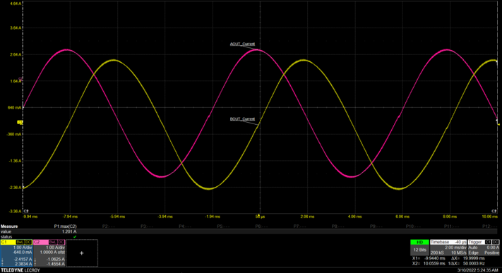
Figure 7-21 shows the smooth sinusoidal coil current waveforms when the motor operates in silent step decay mode.
 Figure 7-21 Coil Current Waveform with Silent Step Decay. Traces from top to bottom: coil A current, coil B current
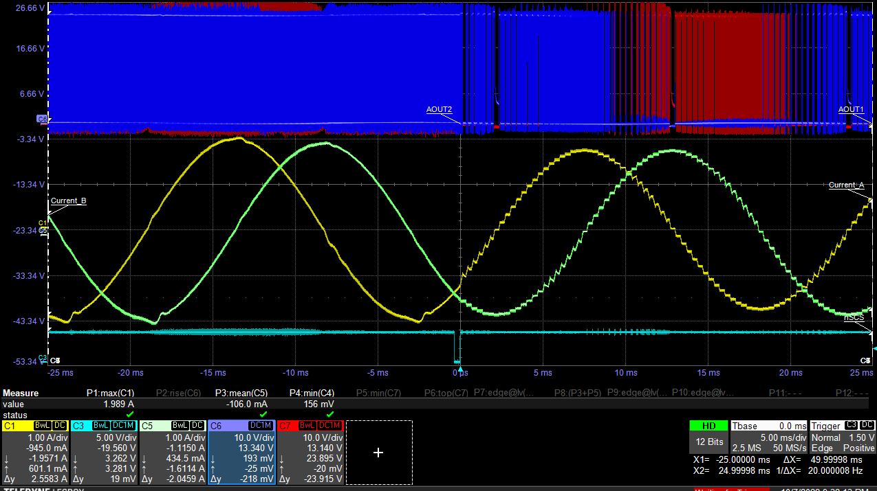
The SS_SMPL_SEL bits influence the smoothness of current waveform around zero crossing point. Default value of 2 μs sampling time will work well for most motors and applications. In case current waveform distortion is oberved around the zero crossing, the value of sampling time can be increased to a maximum of 5 μs. Figure 7-22 an example of transition from silent step decay mode to smart tune ripple control decay mode with a sampling time of 5 μs.
 Figure 7-22 Silent step to smart tune transition. Traces from top to bottom: AOUT2, AOUT1, coil A current, coil B current, nSCS