SLLSFB6B May 2020 – May 2024 DRV8705-Q1
PRODUCTION DATA
- 1
- 1 Features
- 2 Applications
- 3 Descriptions
- Device Comparison Table
- 4 Pin Configuration
- 5 Specifications
-
6 Detailed Description
- 6.1 Overview
- 6.2 Functional Block Diagram
- 6.3
Feature Description
- 6.3.1 External Components
- 6.3.2 Device Interface Variants
- 6.3.3 Input PWM Modes
- 6.3.4 Smart Gate Driver
- 6.3.5 Doubler (Single-Stage) Charge Pump
- 6.3.6 Low-Side Differential Current Shunt Amplifier
- 6.3.7 Pin Diagrams
- 6.3.8
Protection and Diagnostics
- 6.3.8.1 Gate Driver Disable and Enable (DRVOFF and EN_DRV)
- 6.3.8.2 Fault Reset (CLR_FLT)
- 6.3.8.3 DVDD Logic Supply Power on Reset (DVDD_POR)
- 6.3.8.4 PVDD Supply Undervoltage Monitor (PVDD_UV)
- 6.3.8.5 PVDD Supply Overvoltage Monitor (PVDD_OV)
- 6.3.8.6 VCP Charge Pump Undervoltage Lockout (VCP_UV)
- 6.3.8.7 MOSFET VDS Overcurrent Protection (VDS_OCP)
- 6.3.8.8 Gate Driver Fault (VGS_GDF)
- 6.3.8.9 Thermal Warning (OTW)
- 6.3.8.10 Thermal Shutdown (OTSD)
- 6.3.8.11 Offline Short Circuit and Open Load Detection (OOL and OSC)
- 6.3.8.12 Fault Detection and Response Summary Table
- 6.4 Device Function Modes
- 6.5 Programming
- 7 Register Maps
- 8 Application and Implementation
- 9 Power Supply Recommendations
- 10Layout
- 11Device and Documentation Support
- 12Revision History
- 13Mechanical, Packaging, and Orderable Information
Package Options
Refer to the PDF data sheet for device specific package drawings
Mechanical Data (Package|Pins)
- RHB|32
Thermal pad, mechanical data (Package|Pins)
- RHB|32
Orderable Information
6.5.3 SPI Interface for Multiple Slaves
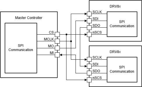
Multiple DRV8705-Q1 devices can be connected to the master controller with and without the daisy chain. For connecting a 'n' number of DRV8705-Q1 to a master controller without using a daisy chain, 'n' number of I/O resources from master controller has to utilized for nSCS pins as shown in Figure 6-21. Whereas, if the daisy chain configuration is used, then a single nSCS line can be used for connecting multiple DRV8705-Q1 devices. Figure 6-22
 Figure 6-21 SPI Operation Without Daisy Chain
 Figure 6-22 SPI Operation With Daisy Chain