SLOSE71 April   2020  – December 2020 DRV8955

PRODUCTION DATA  

  1. Features
  2. Applications
  3. Description
  4. Revision History
  5. Pin Configuration and Functions
    1.     Pin Functions
  6. Specifications
    1. 6.1 Absolute Maximum Ratings
    2. 6.2 ESD Ratings
    3. 6.3 Recommended Operating Conditions
    4. 6.4 Thermal Information
    5. 6.5 Electrical Characteristics
      1. 6.5.1 Typical Characteristics
  7. Detailed Description
    1. 7.1 Overview
    2. 7.2 Functional Block Diagrams
    3. 7.3 Feature Description
      1. 7.3.1 Configuration Options and Bridge Control
      2. 7.3.2 Current Regulation
      3. 7.3.3 Charge Pump
      4. 7.3.4 Linear Voltage Regulators
      5. 7.3.5 Logic and Quad-Level Pin Diagrams
        1. 7.3.5.1 nFAULT Pin
      6. 7.3.6 Protection Circuits
        1. 7.3.6.1 VM Undervoltage Lockout (UVLO)
        2. 7.3.6.2 VCP Undervoltage Lockout (CPUV)
        3. 7.3.6.3 Overcurrent Protection (OCP)
        4. 7.3.6.4 Thermal Shutdown (OTSD)
        5.       Fault Condition Summary
    4. 7.4 Device Functional Modes
      1. 7.4.1 Sleep Mode (nSLEEP = 0)
      2. 7.4.2 Operating Mode (nSLEEP = 1)
      3. 7.4.3 nSLEEP Reset Pulse
      4.      Functional Modes Summary
  8. Application and Implementation
    1. 8.1 Application Information
    2. 8.2 Typical Application
      1. 8.2.1 Design Requirements
      2. 8.2.2 Detailed Design Procedure
        1. 8.2.2.1 Current Regulation
        2. 8.2.2.2 Power Dissipation and Thermal Calculation
        3. 8.2.2.3 Application Curves
  9. Power Supply Recommendations
    1. 9.1 Bulk Capacitance Sizing
  10. 10Layout
    1. 10.1 Layout Guidelines
    2. 10.2 Layout Example
  11. 11Device and Documentation Support
    1. 11.1 Documentation Support
      1. 11.1.1 Related Documentation
    2. 11.2 Receiving Notification of Documentation Updates
    3. 11.3 Support Resources
    4. 11.4 Trademarks
    5. 11.5 Electrostatic Discharge Caution
    6. 11.6 Glossary
  12. 12Mechanical, Packaging, and Orderable Information

Package Options

Mechanical Data (Package|Pins)
Thermal pad, mechanical data (Package|Pins)
Orderable Information

Description

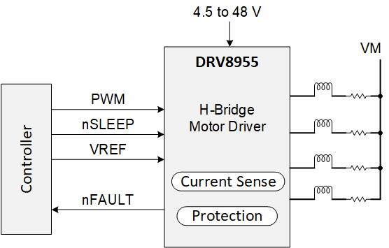
The DRV8955 provides four individually controllable half-bridge drivers for industrial applications. The device can be used for driving up to four solenoid loads, two DC motors, one stepper motor, or other loads.

The output driver for each channel consists of N-channel power MOSFET’s configured in a half-bridge. A simple PWM (IN/IN) interface allows easy interface with the controller. Separate inputs to independently control each half-bridge are provided. Additionally, the outputs can be paralleled together to provide more current for output loads.

The DRV8955 operates off a single power supply and supports a wide input supply range from 4.5 V to 48 V. A low-power sleep mode is provided to achieve a low quiescent current draw by shutting down much of the internal circuitry. Internal protection functions are provided for undervoltage-lockout, overcurrent protection on each FET, short circuit protection, and overtemperature. Fault conditions are indicated by the nFAULT pin.

Device Information
PART NUMBER (1)PACKAGEBODY SIZE (NOM)
DRV8955PPWPRHTSSOP (28)9.7mm x 4.4mm
DRV8955PRGERVQFN (24)4.0mm x 4.0mm
For all available packages, see the orderable addendum at the end of the data sheet.
GUID-DF543B40-C37C-4212-91C0-300520FD867E-low.gifDRV8955 Simplified Schematic