SNLS461A May 2013 – June 2015 DS110DF111
PRODUCTION DATA.
- 1 Features
- 2 Applications
- 3 Description
- 4 Revision History
- 5 Pin Configuration and Functions
- 6 Specifications
-
7 Detailed Description
- 7.1 Overview
- 7.2 Functional Block Diagram
- 7.3 Feature Description
- 7.4 Device Functional Modes
- 7.5
Programming
- 7.5.1
SMBus Interface
- 7.5.1.1 Address Lines
- 7.5.1.2 Device Configuration in SMBus Slave Mode
- 7.5.1.3 Bit Fields in the Register Set
- 7.5.1.4 Writing to and Reading From the Control/Shared Registers
- 7.5.1.5 SMBus Strap Observation
- 7.5.1.6 Interrupt Channel Flag Bits
- 7.5.1.7 Control/Shared Register Reset
- 7.5.1.8 Device Revision and Device ID
- 7.5.1.9 Channel Select Register
- 7.5.1.10 Resetting Individual Channels of the Retimer
- 7.5.1.11 Rate and Subrate Setting
- 7.5.1.12 Overriding the CTLE Boost Setting
- 7.5.1.13 Overriding the Output Multiplexer
- 7.5.1.14 Overriding the VCO Divider Selection
- 7.5.1.15 Using the Internal Eye Opening Monitor
- 7.5.1.16 Overriding the DFE Tap Weights and Polarities
- 7.5.1.17 Enabling Slow Rise/Fall Time on the Output Driver
- 7.5.1.18 Using the PRBS Generator
- 7.5.1.19 Inverting the Output Polarity
- 7.5.1.20 Overriding the Figure of Merit Adaption
- 7.5.1.21 Setting the Rate and Subrate for Lock Acquisition
- 7.5.1.22 Setting the Adaption/Lock Mode
- 7.5.1.23 Initiating Adaption
- 7.5.1.24 Overriding the CTLE Settings used for CTLE Adaption
- 7.5.1.25 Setting the Output Differential Voltage
- 7.5.1.26 Setting the Output De-Emphasis Setting
- 7.5.1.27 CTLE Setting for Divide by 4 and Divide by 8 VCO Ranges
- 7.5.1
SMBus Interface
- 7.6 Register Maps
- 8 Applications and Implementation
- 9 Power Supply Recommendations
- 10Layout
- 11Device and Documentation Support
- 12Mechanical, Packaging, and Orderable Information
Package Options
Mechanical Data (Package|Pins)
- RTW|24
Thermal pad, mechanical data (Package|Pins)
- RTW|24
Orderable Information
8 Applications and Implementation
NOTE
Information in the following applications sections is not part of the TI component specification, and TI does not warrant its accuracy or completeness. TI’s customers are responsible for determining suitability of components for their purposes. Customers should validate and test their design implementation to confirm system functionality.
8.1 Application Information
The DS110DF111 is a 2 channel retimer that support many different data rates and application spaces.
8.2 Typical Application
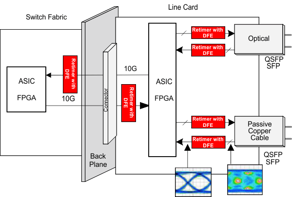
Figure 9 shows a typical implementation for the DS110DF111 in a back plane application. The DS110DF111 can also be used for front port applications. The DS110DF111 supports data rates for CPRI, Infiniband, Ethernet, Interlaken and other custom data rates. For applications which include a lower VCO/4 or VCO/8 data-rate the CTLE value will not adapt automatically. Instead the CTLE value is taken directly from channel register 0x3A. For short, low-loss channels this value should be adjusted as indicated in the Channel Register Table.
 Figure 9. Typical Application
8.2.1 Design Requirements
This section lists some critical areas for high speed printed circuit board design consideration and study.
- Utilize 100-Ω differential impedance traces.
- Back-drill connector vias and signal vias to minimize stub length.
- Use reference plane vias to ensure a low inductance path for the return current.
- Place AC-Coupling capacitors for the transmitter links near the receiver for that channel.
- The maximum body size for AC-coupling capacitors is 0402.
8.2.2 Detailed Design Procedure
To begin the design process determine the following:
- Select a reference clock frequency and routing scheme.
- Plan out channel connectivity. Be sure to note any desired polarity inversion routing in the board schematics.
- Ensure that each device has a unique SMBus address if the control bus is shared with other devices or components.
- Use the IBIS-AMI model for simple channel simulations before PCB layout is complete.
Initialization Sequence: Channel Register Configurations repeated for all desired channels:
- CDR reset
- Adapt Mode Configuration
- Data rate selection
- Output driver VOD and De-Emphasis Optional Interrupt enable
- CDR reset release
8.2.3 Application Curves
8.2.3.1 SFF-8431 Testing
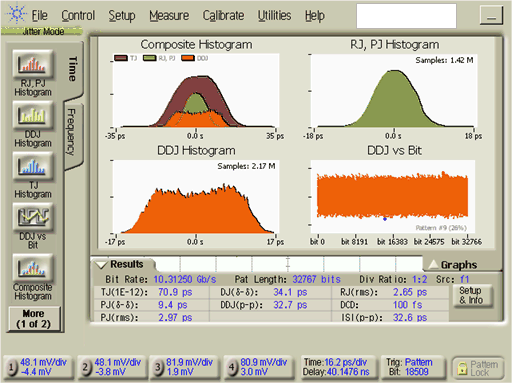
Testing for Receiver Jitter Tolerance based on SFF-8431 section D11.
- Datarate: 10.3125 Gbps
- PRBS15 Pattern
- Output Amplitude: 700 mV
- Periodic Jitter: 70 mUI at 20 MHz
- ISI Jitter: 10" 4-mil FR4 differential microstrip + Limiting Amplifier
- Random Jitter noise source: Agilent 346B
The SFF-8431 specification combines deterministic, random, and periodic jitter components. The combination of these jitter components has been measured and calibrated to ensure adequate levels of individual jitter components and total jitter.
 Figure 10. SFF-8431 Input Jitter Tolerance Profile
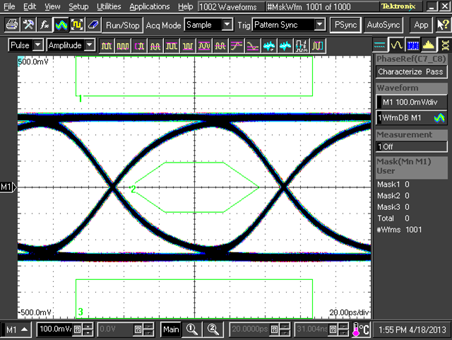
 Figure 11. SFF-8431 Output Jitter Eye Mask
The SFF-8431 specification defines a transmit eye mask to ensure robust signal reception across the host - module interface.