SNLS645A August 2019 – December 2019 DS160PR410
PRODUCTION DATA.
- 1 Features
- 2 Applications
- 3 Description
- 4 Revision History
- 5 Pin Configuration and Functions
- 6 Specifications
- 7 Detailed Description
- 8 Application and Implementation
- 9 Power Supply Recommendations
- 10Layout
- 11Device and Documentation Support
- 12Mechanical, Packaging, and Orderable Information
Package Options
Mechanical Data (Package|Pins)
- RNQ|40
Thermal pad, mechanical data (Package|Pins)
Orderable Information
8.2.1.2 Detailed Design Procedure
In PCIe Gen 4.0 and Gen 3.0 applications, the specification requires Rx-Tx link training to establish and optimize signal conditioning settings at 16 Gbps and 8 Gbps, respectively. In link training, the Rx partner requests a series of FIR – pre-shoot and de-emphasis coefficients (10 Presets) from the Tx partner. The Rx partner includes 7-levels (6 dB to 12 dB) of CTLE followed by a single tap DFE. The link training would pre-condition the signal, with an equalized link between the root-complex and endpoint.
Note that there is no link training in PCIe Gen 1.0 (2.5 Gbps) or PCIe Gen 2.0 (5.0 Gbps) applications. The DS160PR410 is placed in between the Tx and Rx. It helps extend the PCB trace reach distance by boosting the attenuated signals with its equalization, which allows the user to recover the signal by the downstream Rx more easily.
For operation in Gen 4.0 and Gen 3.0 links, the DS160PR410 transmit outputs are designed to pass the Tx Preset signaling onto the Rx for the PCIe Gen 4.0 or Gen 3.0 link to train and optimize the equalization settings. The suggested setting for the DS160PR410 are VOD = 0 dB and DC GAIN = 0 dB. Adjustments to the EQ setting should be performed based on the channel loss to optimize the eye opening in the Rx partner. The available EQ gain settings are provided in Table 1.
The Tx equalization presets or CTLE and DFE coefficients in the Rx can also be adjusted to further improve the eye opening.
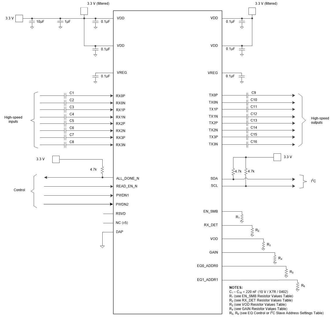
Figure 11 shows as an example for DS160PR410 Typical Connection Schematic.
 Figure 11. DS160PR410 Typical Connection Schematic