SNOSC82B August 2012 – June 2015 DS1776QML
PRODUCTION DATA.
- 1Features
- 2Description
- 3Revision History
- 4Pin Configuration and Functions
-
5Specifications
- 5.1 Absolute Maximum Ratings
- 5.2 ESD Ratings
- 5.3 Recommend Operating Conditions
- 5.4 Thermal Information
- 5.5 Quality Conformance Inspection
- 5.6 Pi Bus Transceiver DS1776 DC Parameters
- 5.7 Pi Bus Transceiver DS1776 AC Parameters: B To A Path
- 5.8 Pi Bus Transceiver DS1776 AC Parameters: A To B Path
- 5.9 Pi Bus Transceiver DS1776 AC Parameters: Setup / Hold / Pulse Width Specifications
- 5.10 Test Circuit And Waveforms
- 6Detailed Description
- 7Device and Documentation Support
- 8Mechanical, Packaging, and Orderable Information
Package Options
Mechanical Data (Package|Pins)
- FK|28
Thermal pad, mechanical data (Package|Pins)
Orderable Information
5 Specifications
5.1 Absolute Maximum Ratings(1)
| MIN | MAX | UNIT | ||
|---|---|---|---|---|
| Supply Voltage (VCC) | −0.5 | 7.0 | V | |
| VX, VOH Output Level Control Voltage (A Outputs) | −0.5 | 7.0 | V | |
| OEBn, OEA, LE Input Voltage (VI) | −0.5 | 7.0 | V | |
| A0–A7, B0–B7 Input Voltage (VI) | −0.5 | 5.5 | V | |
| Input Current (II) | −40 | 5 | mA | |
| Voltage Applied to Output in High Output State (VO) | −0.5V | +VCC | ||
| A0–A7 Current Applied to Output in Low Output State (IO) | 40 | 40 | mA | |
| B0–B7 Current Applied to Output in Low Output State (IO) | 200 | 200 | mA | |
| Lead Temperature (Soldering 10 Sec.) | 260 | °C | ||
| Power Dissipation (2) | 740 | mW | ||
| Storage temperature | Tstg | −65 | +150 | °C |
5.2 ESD Ratings
| MIN | MAX | UNIT | |||
|---|---|---|---|---|---|
| V(ESD) | Electrostatic discharge | Human body model (HBM), per ANSI/ESDA/JEDEC JS-001, all pins(1)(2) | 500 | V | |
(1) JEDEC document JEP155 states that 500-V HBM allows safe manufacturing with a standard ESD control process.
(2) CZap = 120 pF, RZap = 1500Ω
5.3 Recommend Operating Conditions
| MIN | MAX | UNIT | |
|---|---|---|---|
| Supply Voltage (VCC) | 4.5 | 5.5 | V |
| Operating Temp. Range (TA) | −55 | +125 | °C |
5.4 Thermal Information
| THERMAL METRIC(1) | DS1776QML | UNIT | |
|---|---|---|---|
| FK0028A | |||
| 28 PINS | |||
| RθJA | Junction-to-ambient thermal resistance | +67.5 | °C/W |
| RθJC(top) | Junction-to-case (top) thermal resistance | See MIL-STD-1835 | °C/W |
(1) For more information about traditional and new thermal metrics, see the IC Package Thermal Metrics application report, SPRA953.
5.5 Quality Conformance Inspection
Table 1. Mil-Std-883, Method 5005 - Group A
| Subgroup | Description | Temp (°C) |
|---|---|---|
| 1 | Static tests at | +25 |
| 2 | Static tests at | +125 |
| 3 | Static tests at | -55 |
| 4 | Dynamic tests at | +25 |
| 5 | Dynamic tests at | +125 |
| 6 | Dynamic tests at | -55 |
| 7 | Functional tests at | +25 |
| 8A | Functional tests at | +125 |
| 8B | Functional tests at | -55 |
| 9 | Switching tests at | +25 |
| 10 | Switching tests at | +125 |
| 11 | Switching tests at | -55 |
| 12 | Settling time at | +25 |
| 13 | Settling time at | +125 |
| 14 | Settling time at | -55 |
5.6 Pi Bus Transceiver DS1776 DC Parameters
The following conditions apply, unless otherwise specified. VCC = 5.5V| SYMBOL | PARAMETER | CONDITIONS | NOTES | MIN | MAX | UNIT | SUB- GROUPS |
|---|---|---|---|---|---|---|---|
| VIL2 | Low Level In Voltage Bn | VCC = 4.5 | See(3) | 1.45 | V | 1, 2, 3 | |
| VIL1 | All Other Inputs | VCC = 4.5 | .8 | V | 1, 2, 3 | ||
| VIH1 | Hi Level Input Voltage OEBn, OEA, An, LE | See(3) | 2.0 | V | 1, 2, 3 | ||
| VIH2 | High Level In Voltage B0-B7 | 1.6 | V | 1, 2, 3 | |||
| IOH1 | High Level Output Current An | VCC = 4.5, VIN = VIH or VIL, VOH = 2.5V |
See(4) | -3.0 | mA | 1, 2, 3 | |
| IOH2 | High Level Output Current Bn | VCC = 5.5, VIL = 0.8V, VIH = 2.0V, VOH = 2.1V |
100 | µA | 1, 2, 3 | ||
| IOL1 | Low Level Output Current An | VCC = 4.5, VIN = VIH or VIL, VOL = 0.5V |
See(5) | 20 | mA | 1, 2, 3 | |
| IOL2 | Low Level Output Current Bn | VCC = 4.5, VIN = VIH or VIL, VOL = 1.15V |
100 | mA | 1, 2, 3 | ||
| VOH | High Level Output Voltage An | VCC = 4.5, VIN = VIL or VIH, IOH = -3 mA, VX = 4.5V |
2.5 | 4.5 | V | 1, 2, 3 | |
| VCC = 4.5, VIN = VIL or VIH, IOH = -0.4 mA, VX = 3.13 to 3.47V |
2.5 | VX | V | 1, 2, 3 | |||
| VOL | Low Level Output Voltage An | VCC = 4.5, VIL = Max, VIH = Min, IOL = 20mA, VX = VCC |
0.5 | V | 1, 2, 3 | ||
| VOLB | Low Level Output Voltage Bn | VCC = 4.5, VIL = Max, VIH = Min, IOL = 100mA |
1.15 | V | 1, 2, 3 | ||
| VCC = 4.5, VIL = Max, VIH = Min, IOL = 4mA |
0.4 | V | 1, 2, 3 | ||||
| VIK | Input Clamp Voltage An | VCC = 4.5, II = -40mA | -0.5 | V | 1, 2, 3 | ||
| VIK | Input Clamp Voltage Other Inputs | VCC = 4.5, II = -18mA | -1.2 | V | 1, 2, 3 | ||
| IIH1 | Input Current Max Input Voltage OEBn, OEA, LE | VCC = 5.5, VI = 7.0V | 100 | µA | 1, 2, 3 | ||
| IIH2 | Input Current Max Input Voltage An, Bn | VCC = 5.5, VI = 5.5V | 1.0 | mA | 1, 2, 3 | ||
| IIH3 | High Level Input Current OEBn, OEA, LE | VCC = 5.5, VI = 2.7V | 20 | µA | 1, 2, 3 | ||
| IIH4 | High Level Input Current Bn | VCC = 5.5, VI = 2.1V | 100 | µA | 1, 2, 3 | ||
| IIL1 | Low Level Input Current OEBn, OEA, Except OEBn or OEA | VCC = 5.5, VI = 0.5V | -20 | µA | 1, 2, 3 | ||
| IIL2 | Low Level Input Current LE | VCC = 5.5, VI = 0.5V | -20 | µA | 1 | ||
| -40 | µA | 2, 3 | |||||
| IIL3 | Low Level Input Current Bn | VCC = 5.5, VI = 0.3V | -100 | µA | 1, 2, 3 | ||
| IOZH + IIH | TRI-STATE Output Current, High Level Voltage Applied An | VCC = 5.5, VO = 2.7V | 70 | µA | 1, 2, 3 | ||
| IOZL + IIL | TRI-STATE Output Current, Low Level Voltage Applied An | VCC = 5.5, VO = 0.5V | -70 | µA | 1, 2, 3 | ||
| IX | High Level Control Current | VCC = 5.5, VX = 5.5V, LE = OEA = OEBn = 2.7V, A0-A7 = 2.7, B0-B7 = 2V |
-100 | 100 | µA | 1, 2, 3 | |
| VCC = 5.5, B0-B7 = 2V VX = 3.13V and 3.47V, LE = OEA = 2.7V, OEBn = A0-A7 = 2.7V, |
-10 | 10 | mA | 1, 2, 3 | |||
| IOS | Short Circuit Output Current A0-A7 only | VCC = 5.5, Bn = 1.9V, OEA = 2.0V, OEBn = 2.7V, VO = 0V |
See(6) | -60 | -150 | mA | 1, 2, 3 |
| ICCH | Supply Current (Total) ICCH | VCC = 5.5, VIN (An) = 5.0V | 37 | mA | 1, 2 | ||
| 41 | mA | 3 | |||||
| ICCL | Supply Current (Total) ICCL | VCC = 5.5, VIN (An) = 0.5V | 38 | mA | 1, 3 | ||
| 34 | mA | 2 | |||||
| ICCZ | Supply Current (Total) ICCZ | VCC = 5.5, VIN (An) = 0.5V | 35 | mA | 1, 2, 3 | ||
| IOff | Power Off Output Current B0-B7 | VCC = 0, Bn = 2.1V, VIL = Max, VIH = Min |
100 | µA | 1, 2, 3 |
5.7 Pi Bus Transceiver DS1776 AC Parameters: B To A Path
The following conditions apply, unless otherwise specified. VCC = 5V ±10%, CL = 50pF, RL = 500Ω| SYMBOL | PARAMETER | CONDITIONS | NOTES | MIN | MAX | UNIT | SUB- GROUPS |
|---|---|---|---|---|---|---|---|
| tPLH | Propagation Delay B to A | Waveform 1, 2 | 4.5 | 17 | ns | 9, 10, 11 | |
| tPHL | Propagation Delay B to A | Waveform 1, 2 | 6.0 | 17 | ns | 9, 10, 11 | |
| tPZH | Output Enable OEA To A | Waveform 3, 4 | 4.0 | 17 | ns | 9, 10, 11 | |
| tPZL | Output Enable OEA To A | Waveform 3, 4 | 4.0 | 21 | ns | 9, 10, 11 | |
| tPHZ | Output Disable OEA to A | Waveform 3, 4 | 2.0 | 12 | ns | 9, 10, 11 | |
| tPLZ | Output Disable OEA to A | Waveform 3, 4 | 2.0 | 13 | ns | 9, 10, 11 |
5.8 Pi Bus Transceiver DS1776 AC Parameters: A To B Path
The following conditions apply, unless otherwise specified. VCC = 5V ±10%, CL = 30pF, RL = 9Ω| SYMBOL | PARAMETER | CONDITIONS | NOTES | MIN | MAX | UNIT | SUB- GROUPS |
|---|---|---|---|---|---|---|---|
| tPLH | Propagation Delay A to B | Waveform 1, 2 | 2.0 | 13 | ns | 9, 11 | |
| 2.0 | 17 | ns | 10 | ||||
| tPHL | Propagation Delay A to B | Waveform 1, 2 | 2.5 | 13 | ns | 9, 10, 11 | |
| tPLH | Propagation Delay LE to B | Waveform 1, 2 | 2.0 | 16 | ns | 9, 11 | |
| 2.0 | 22 | ns | 10 | ||||
| tPHL | Propagation Delay LE to B | Waveform 1, 2 | 2.0 | 16 | ns | 9, 10, 11 | |
| tPLH | Enable / Disable Time OEBn to B | Waveform 1, 2 | 2.0 | 13 | ns | 9, 11 | |
| 2.0 | 16 | ns | 10 | ||||
| tPHL | Enable / Disable Time OEBn to B | Waveform 1, 2 | 3.5 | 14 | ns | 9 | |
| 3.5 | 13 | ns | 10 | ||||
| 3.5 | 16 | ns | 11 |
5.9 Pi Bus Transceiver DS1776 AC Parameters: Setup / Hold / Pulse Width Specifications
The following conditions apply, unless otherwise specified. VCC = 5V ±10%| SYMBOL | PARAMETER | CONDITIONS | NOTES | MIN | MAX | UNIT | SUB- GROUPS |
|---|---|---|---|---|---|---|---|
| tS | A to LE Setup | Waveform 5 | 7.0 | ns | 9, 10, 11 | ||
| tH | A to LE Hold | Waveform 5 | 0.0 | ns | 9, 10, 11 | ||
| tW | LE Pulse Width Low | Waveform 5 | 12 | ns | 9, 10, 11 |
(1) Absolute Maximum Ratings indicate limits beyond which damage to the device may occur. Operating Ratings indicate conditions for which the device is functional, but do not guarantee specific performance limits. For specified specifications and test conditions, see the Electrical Characteristics. The specified specifications apply only for the test conditions listed. Some performance characteristics may degrade when the device is not operated under the listed test conditions.
(2) The maximum power dissipation must be derated at elevated temperatures and is dictated by TJmax (maximum junction temperature), θJA (package junction to ambient thermal resistance), and TA (ambient temperature). The maximum allowable power dissipation at any temperature is PDmax = (TJmax - TA)/θJA or the number given in the Absolute Maximum Ratings, whichever is lower.
(3) Tested Go-No-Go
(4) Same as VOH test.
(5) Same as VOL test.
(6) Not more than one output should be shorted at a time. For testing IOS, the use of high speed test apparatus and/or sample-and-hold techniques are preferable in order to minimize internal heating and more accurately reflect operational values. Otherwise, prolonged shorting of a High output may raise the chip temperature above normal and thereby cause invalid readings in other parameter tests. In any sequence of parameter test, IOS tests should be performed last.
 Figure 1. Propagation Delay For Data To Output
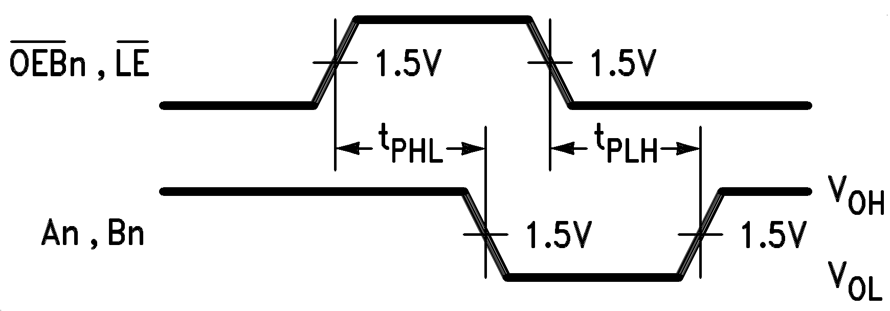 Figure 2. Propagation Delay For Data To Output
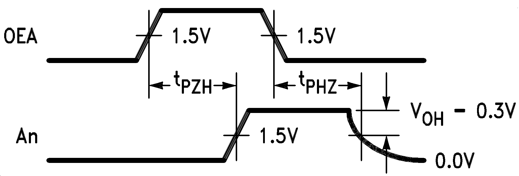 Figure 3. TRI-STATE Output Enable Time
To High Level And Output Disable
Time From High Level
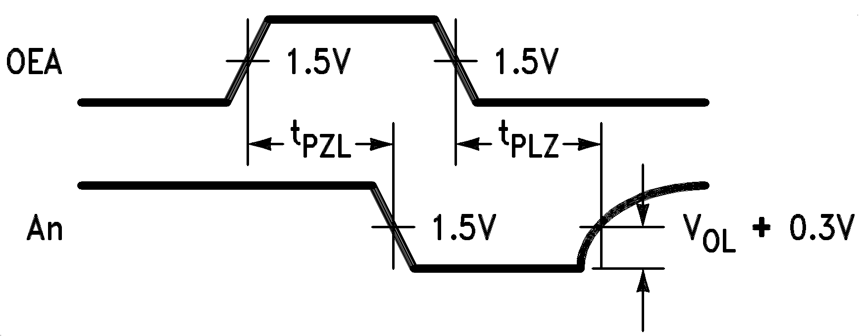 Figure 4. TRI-STATE Output Enable Time
To Low Level And Output Disable
Time From Low Level

The shaded areas indicate when the input is permitted to change for predictable output performance.
Figure 5. Data Setup And Hold Times And Le Pulse Widths
5.10 Test Circuit And Waveforms
5.10.1 Test Circuit For TRI-STATE Outputs On A Side
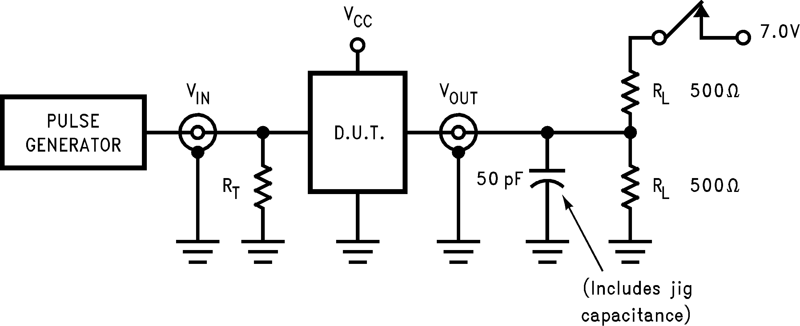
Table 2. Switch Position
| Test | Switch |
|---|---|
| tPLZ, tPZL | Closed |
| All Other | Open |
5.10.2 Test Circuit For TRI-STATE Outputs On B Side
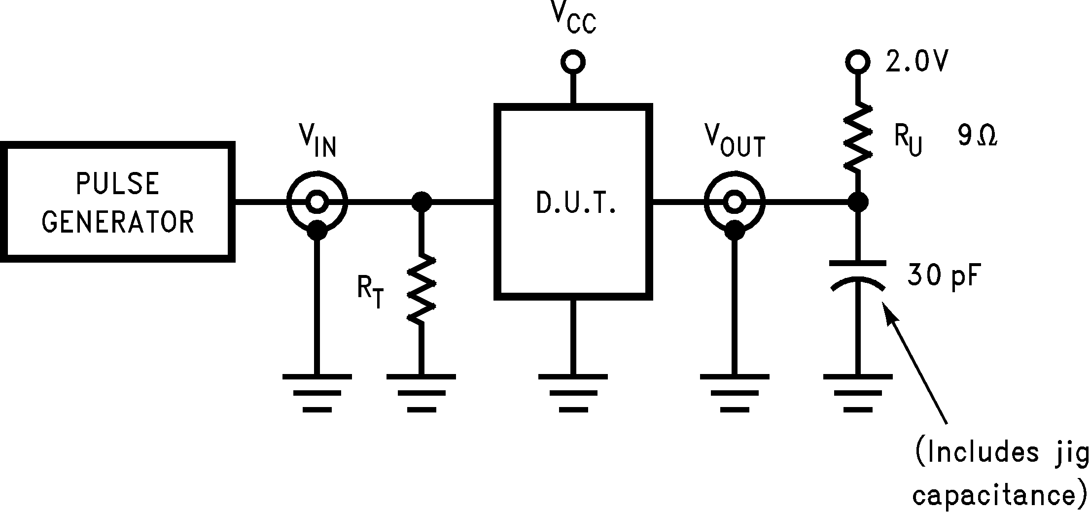
DEFINITIONS
RL = Load resistor 500Ω
CL = Load capacitance includes jig and probe capacitance
RT = Termination resistance should be equal to ZO of pulse generators.
RU = Pull up resistor
RL = Load resistor 500Ω
CL = Load capacitance includes jig and probe capacitance
RT = Termination resistance should be equal to ZO of pulse generators.
RU = Pull up resistor
5.10.3 Input Pulse Definition
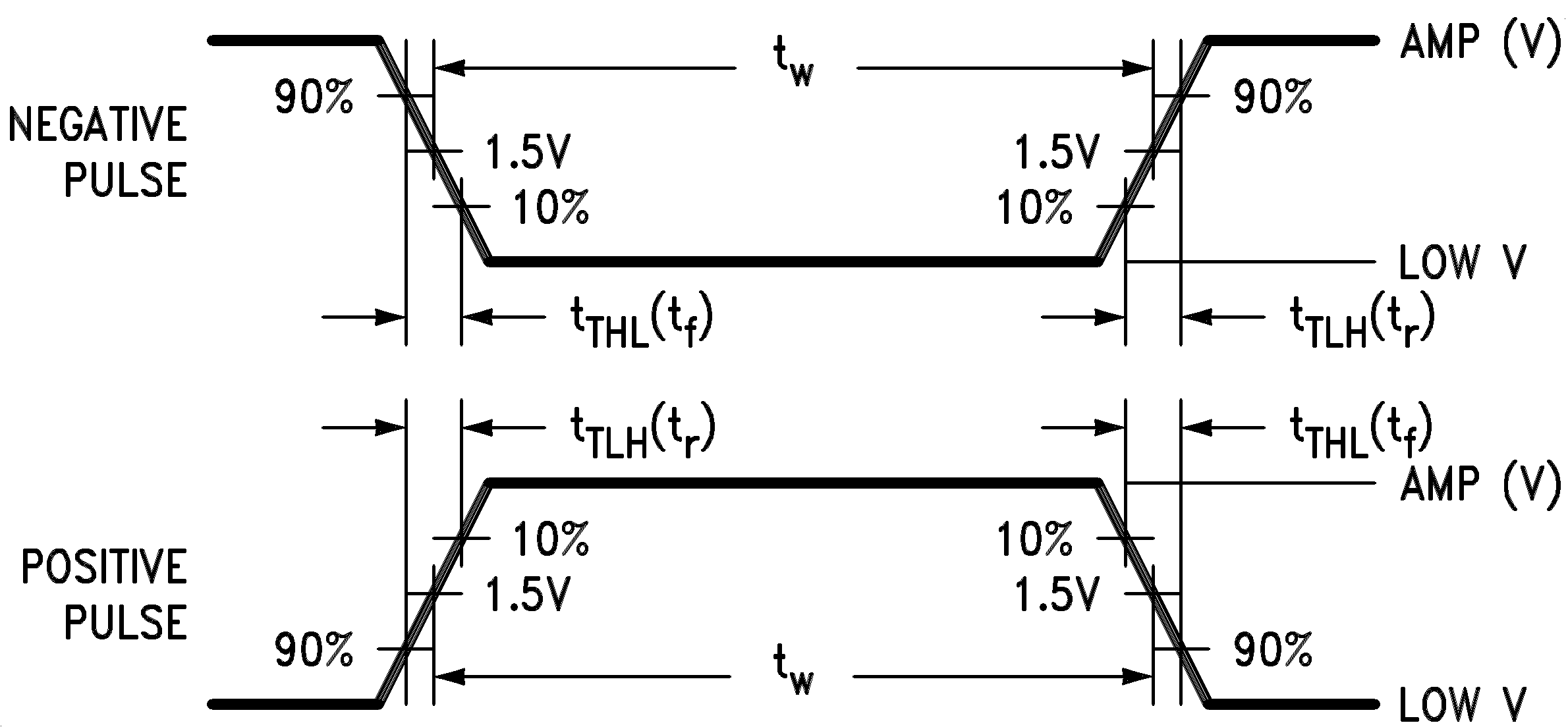
| Input Pulse Characteristics | ||||||
|---|---|---|---|---|---|---|
| Amplitude | Low V | Rep. Rate | tW | tTLH | tTHL | |
| A Side | 3.0V | 0.0V | 1 MHz | 500 ns | 2 ns | 2 ns |
| B Side | 2.0V | 1.0V | 1 MHz | 500 ns | 2 ns | 2 ns |