SNLS561B February   2017  – October 2019 DS250DF210

PRODUCTION DATA.  

  1. Features
  2. Applications
  3. Description
    1.     Device Images
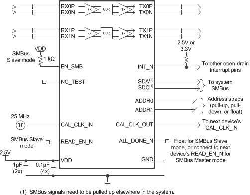
      1.      Simplified Schematic
  4. Revision History
  5. Description (continued)
  6. Pin Configuration and Functions
    1.     Pin Functions
  7. Specifications
    1. 7.1  Absolute Maximum Ratings
    2. 7.2  ESD Ratings
    3. 7.3  Recommended Operating Conditions
    4. 7.4  Thermal Information
    5. 7.5  Electrical Characteristics
    6. 7.6  Timing Requirements, Retimer Jitter Specifications
    7. 7.7  Timing Requirements, Retimer Specifications
    8. 7.8  Timing Requirements, Recommended Calibration Clock Specifications
    9. 7.9  Recommended SMBus Switching Characteristics (Slave Mode)
    10. 7.10 Recommended SMBus Switching Characteristics (Master Mode)
    11. 7.11 Typical Characteristics
  8. Detailed Description
    1. 8.1 Overview
    2. 8.2 Functional Block Diagram
    3. 8.3 Feature Description
      1. 8.3.1  Device Data Path Operation
      2. 8.3.2  Signal Detect
      3. 8.3.3  Continuous Time Linear Equalizer (CTLE)
      4. 8.3.4  Variable Gain Amplifier (VGA)
      5. 8.3.5  Cross-Point Switch
      6. 8.3.6  Decision Feedback Equalizer (DFE)
      7. 8.3.7  Clock and Data Recovery (CDR)
      8. 8.3.8  Calibration Clock
      9. 8.3.9  Differential Driver With FIR Filter
        1. 8.3.9.1 Setting the Output VOD, Precursor, and Postcursor Equalization
        2. 8.3.9.2 Output Driver Polarity Inversion
      10. 8.3.10 Debug Features
        1. 8.3.10.1 Pattern Generator
        2. 8.3.10.2 Pattern Checker
        3. 8.3.10.3 Eye Opening Monitor
      11. 8.3.11 Interrupt Signals
    4. 8.4 Device Functional Modes
      1. 8.4.1 Supported Data Rates
      2. 8.4.2 SMBus Master Mode
      3. 8.4.3 Device SMBus Address
    5. 8.5 Programming
      1. 8.5.1 Bit Fields in the Register Set
      2. 8.5.2 Writing to and Reading from the Global/Shared/Channel Registers
    6. 8.6 Register Maps
  9. Application and Implementation
    1. 9.1 Application Information
    2. 9.2 Typical Applications
      1. 9.2.1 Front-Port Jitter Cleaning Applications
        1. 9.2.1.1 Design Requirements
        2. 9.2.1.2 Detailed Design Procedure
      2. 9.2.2 Active Cable Applications
        1. 9.2.2.1 Design Requirements
        2. 9.2.2.2 Detailed Design Procedure
      3. 9.2.3 Backplane and Mid-Plane Applications
      4. 9.2.4 Design Requirements
      5. 9.2.5 Detailed Design Procedure
      6. 9.2.6 Application Curves
  10. 10Power Supply Recommendations
  11. 11Layout
    1. 11.1 Layout Guidelines
    2. 11.2 Layout Example
  12. 12Device and Documentation Support
    1. 12.1 Device Support
      1. 12.1.1 Development Support
    2. 12.2 Documentation Support
      1. 12.2.1 Related Documentation
    3. 12.3 Receiving Notification of Documentation Updates
    4. 12.4 Support Resources
    5. 12.5 Trademarks
    6. 12.6 Electrostatic Discharge Caution
    7. 12.7 Glossary
  13. 13Mechanical, Packaging, and Orderable Information

Package Options

Mechanical Data (Package|Pins)
Thermal pad, mechanical data (Package|Pins)
Orderable Information

Device Images

Simplified Schematic
DS250DF210 DS250DF200_simplified_schematic.gif