SNLS144K June 2005 – March 2024 DS40MB200
PRODUCTION DATA
- 1
- 1 Features
- 2 Applications
- 3 Description
- 4 Pin Configuration and Functions
- 5 Specifications
- 6 Parameter Measurement Information
- 7 Detailed Description
- 8 Application and Implementation
- 9 Power Supply Recommendations
- 10Layout
- 11Device and Documentation Support
- 12Revision History
- 13Mechanical, Packaging, and Orderable Information
Package Options
Mechanical Data (Package|Pins)
- NJU|48
Thermal pad, mechanical data (Package|Pins)
Orderable Information
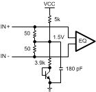
7.3.1 CML Inputs and EQ
The high-speed inputs are self-biased to about 1.3 V at IN+ and IN- and are designed for AC coupling. See Reciever Input Termination and Bias Circuit for details about the internal receiver input termination and bias circuit.
 Figure 7-1 Receiver Input Termination and Bias Circuit
The inputs are compatible to most AC coupling differential signals such as LVDS, LVPECL, and CML. The DS40MB200 is not designed to operate with data rates below 1000 Mbps or with a DC bias applied to the CML inputs or outputs. Most high-speed links are encoded for DC balance and have been defined to include AC coupling capacitors, allowing the DS40MB200 to be inserted directly into the datapath without any limitation. The ideal AC-coupling capacitor value is often based on the lowest frequency component embedded within the serial link. A typical AC-coupling capacitor value ranges between 100 and 1000 nF. Some specifications with scrambled data may require a larger capacitor for optimal performance. To reduce unwanted parasitic effects around and within the AC-coupling capacitor, a body size of 0402 is recommended. AC Test Circuit shows the AC-coupling capacitor placement in an AC test circuit.
Each input stage has a fixed equalizer that provides equalization to compensate about 5 dB (at 2 GHz) of transmission loss from a short backplane trace (about 10 inches backplane).