SNLS144K June 2005 – March 2024 DS40MB200
PRODUCTION DATA
- 1
- 1 Features
- 2 Applications
- 3 Description
- 4 Pin Configuration and Functions
- 5 Specifications
- 6 Parameter Measurement Information
- 7 Detailed Description
- 8 Application and Implementation
- 9 Power Supply Recommendations
- 10Layout
- 11Device and Documentation Support
- 12Revision History
- 13Mechanical, Packaging, and Orderable Information
Package Options
Mechanical Data (Package|Pins)
- NJU|48
Thermal pad, mechanical data (Package|Pins)
Orderable Information
3 Description
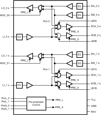
The DS40MB200 device is a dual signal conditioning 2:1 multiplexer (MUX) and 1:2 fan-out buffer designed for use in backplane-redundancy applications. Signal conditioning features include continuous time linear equalization (CTLE) and programmable output pre-emphasis, extending data communication in FR4 backplanes at rates up to 4 Gbps. Each input stage has a fixed equalizer to reduce intersymbol interference distortion from board traces.
All output drivers have four selectable steps of pre-emphasis to compensate for transmission losses from long FR4 backplanes and reduce deterministic jitter. The pre-emphasis levels can be independently controlled for the line-side and switch-side drivers. The internal loopback paths from switch-side input to switch-side output enable at-speed system testing. All receiver inputs are internally terminated with 100-Ω differential terminating resistors. All drivers are internally terminated with 50 Ω to VCC.
| PART NUMBER | PACKAGE(1) | BODY SIZE (NOM) |
|---|---|---|
| DS40MB200 | WQFN (48) | 7.00 mm × 7.00 mm |
