SNLS144K June 2005 – March 2024 DS40MB200
PRODUCTION DATA
- 1
- 1 Features
- 2 Applications
- 3 Description
- 4 Pin Configuration and Functions
- 5 Specifications
- 6 Parameter Measurement Information
- 7 Detailed Description
- 8 Application and Implementation
- 9 Power Supply Recommendations
- 10Layout
- 11Device and Documentation Support
- 12Revision History
- 13Mechanical, Packaging, and Orderable Information
Package Options
Mechanical Data (Package|Pins)
- NJU|48
Thermal pad, mechanical data (Package|Pins)
Orderable Information
5.6 Switching Characteristics
over operating free-air temperature range (unless otherwise noted)
| PARAMETER | TEST CONDITIONS | MIN | TYP(1) | MAX | UNIT | |
|---|---|---|---|---|---|---|
| tR | Differential low-to-high transition time | Measured with a clock-like
pattern at 100 MHz, between 20% and 80% of the differential output
voltage. Pre-emphasis disabled. Transition time is measured with fixture as shown in AC Test Circuit, adjusted to reflect the transition time at the output pins. | 80 | ps | ||
| tF | Differential high-to-low transition time | 80 | ps | |||
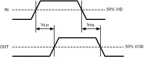
| tPLH | Differential low-to-high propagation delay | Measured at 50% differential voltage from input to output. | 0.5 | 2 | ns | |
| tPHL | Differential high-to-low propagation delay | 0.5 | 2 | ns | ||
| tSKP | Pulse skew(2) | |tPHL–tPLH| | 20 | ps | ||
| tSKO | Output skew(3)(2) | Difference in propagation delay among data paths in the same device. | 200 | ps | ||
| tSKPP | Part-to-part skew(2) | Difference in propagation delay between the same output from devices operating under identical condition. | 500 | ps | ||
| tSM | MUX switch time | Measured from VIH or VIL of the mux-control or loopback control to 50% of the valid differential output. | 1.8 | 6 | ns | |
(1) Typical parameters measured at VCC = 3.3 V, TA = 25°C. They are for reference purposes and are not production-tested.
(2) Specified by design and characterization using statistical analysis.
(3) tSKO is the magnitude difference in the propagation delays among data paths between switch A and switch B of the same port and similar data paths between port 0 and port 1. An example is the output skew among data paths from SIA_0± to LO_0±, SIB_0± to LO_0±, SIA_1± to LO_1± and SIB_1± to LO_1±. Another example is the output skew among data paths from LI_0± to SOA_0±, LI_0± to SOB_0±, LI_1± to SOA_1± and LI_1± to SOB_1±. tSKO also refers to the delay skew of the loopback paths of the same port and between similar data paths between port 0 and port 1. An example is the output skew among data paths SIA_0± to SOA_0±, SIB_0± to SOB_0±, SIA_1± to SOA_1± and SIB_1± to SOB_1±.
 Figure 5-1 Driver Output Transition Time
 Figure 5-2 Propagation Delay From Input to Output
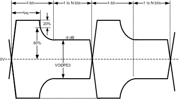
 Figure 5-3 Test Condition for Output Pre-Emphasis Duration