SNLS144K June 2005 – March 2024 DS40MB200
PRODUCTION DATA
- 1
- 1 Features
- 2 Applications
- 3 Description
- 4 Pin Configuration and Functions
- 5 Specifications
- 6 Parameter Measurement Information
- 7 Detailed Description
- 8 Application and Implementation
- 9 Power Supply Recommendations
- 10Layout
- 11Device and Documentation Support
- 12Revision History
- 13Mechanical, Packaging, and Orderable Information
Package Options
Mechanical Data (Package|Pins)
- NJU|48
Thermal pad, mechanical data (Package|Pins)
Orderable Information
10.2 Layout Examples
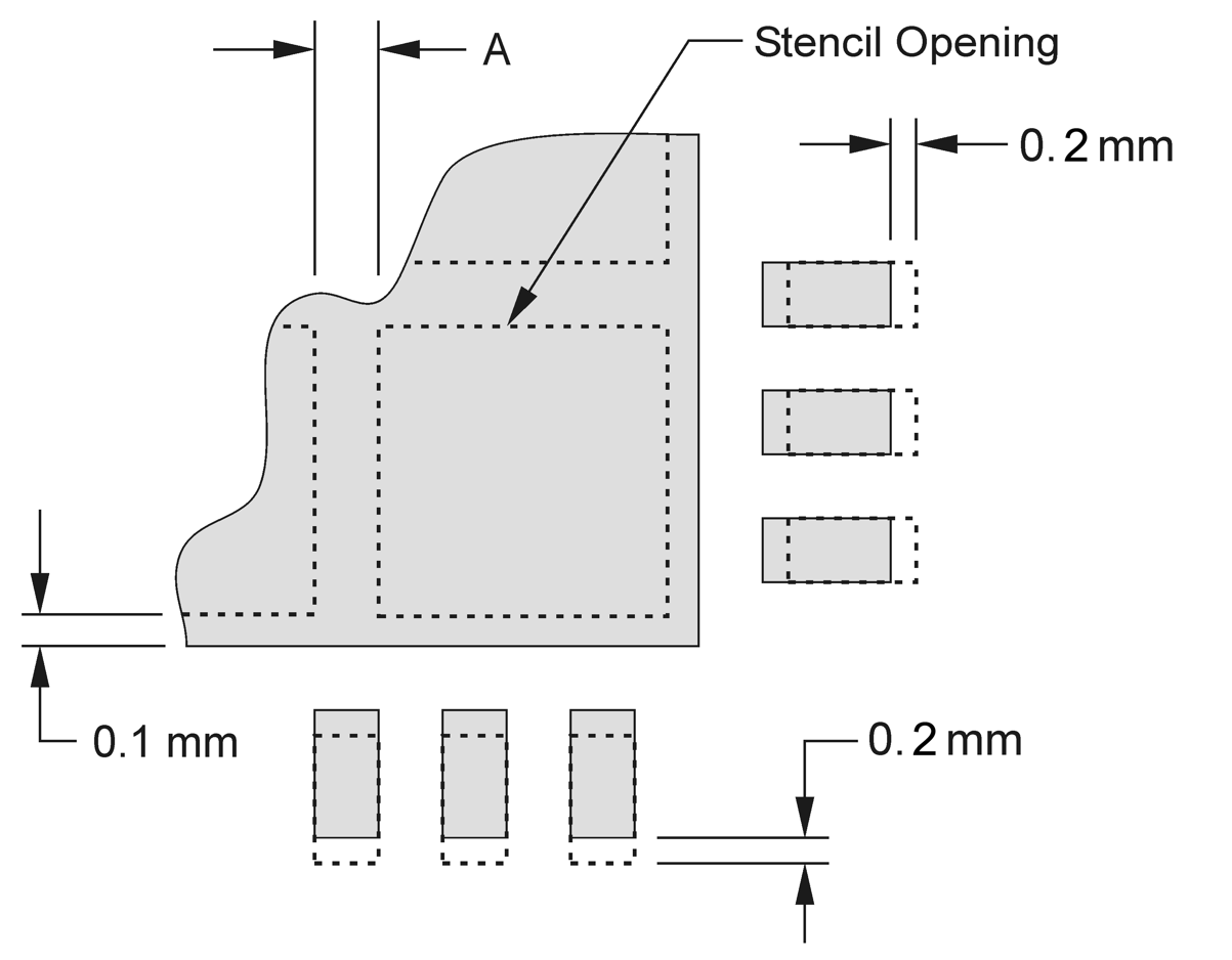
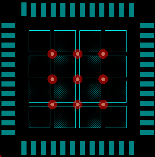
Stencil parameters such as aperture area ratio and the fabrication process have a significant impact on paste deposition. Inspection of the stencil prior to placement of the WQFN package is highly recommended to improve board assembly yields. If the via and aperture openings are not carefully monitored, the solder may flow unevenly through the DAP. Stencil parameters for aperture opening and via locations are shown in Figure 10-1. A layout example for the DS40MB200 DAP is shown in Figure 10-2, where 16 stencil openings are used for the DAP alongside nine vias to GND.
 Figure 10-1 No Pullback WQFN, Single Row Reference Diagram
Table 10-1 No Pullback WQFN Stencil Aperture Summary for DS40MB200
| DEVICE | PIN COUNT | MKT DWG | PCB I/O PAD SIZE (mm) | PCB PITCH (mm) | PCB DAP SIZE (mm) | STENCIL I/O APERTURE (mm) | STENCIL DAP APERTURE (mm) | NUMBER OF DAP APERTURE OPENINGS | GAP BETWEEN DAP APERTURE (Dim A mm) |
|---|---|---|---|---|---|---|---|---|---|
| DS40MB200 | 48 | SQA48A | 0.25 × 0.6 | 0.5 | 5.1 × 5.1 | 0.25 × 0.7 | 1.1 × 1.1 | 16 | 0.2 |
 Figure 10-2 48-Pin WQFN Stencil Example of Via and Opening Placement