SNLS401C February 2012 – September 2018 DS90C187
PRODUCTION DATA.
- 1 Features
- 2 Applications
- 3 Description
- 4 Revision History
- 5 Description (continued)
- 6 Pin Configuration and Functions
- 7 Specifications
-
8 Detailed Description
- 8.1 Overview
- 8.2 Functional Block Diagrams
- 8.3
Device Functional Modes
- 8.3.1 Device Configuration
- 8.3.2 Single Pixel Input / Single Pixel Output
- 8.3.3 Single Pixel Input / Dual Pixel Output
- 8.3.4 Dual Pixel Input / Dual Pixel Output
- 8.3.5 Pixel Clock Edge Select (RFB)
- 8.3.6 Power Management
- 8.3.7 Sleep Mode (PDB)
- 8.3.8 LVDS Outputs
- 8.3.9 18 bit / 24 bit Color Mode (18B)
- 8.3.10 LVCMOS Inputs
- 8.4 Programming
- 9 Application and Implementation
- 10Power Supply Recommendations
- 11Layout
- 12Device and Documentation Support
- 13Mechanical, Packaging, and Orderable Information
Package Options
Mechanical Data (Package|Pins)
- NLA|92
Thermal pad, mechanical data (Package|Pins)
Orderable Information
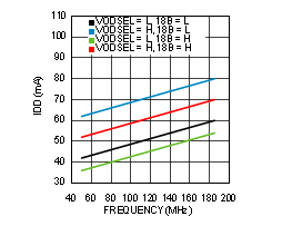
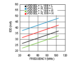
7.9 Typical Characteristics
 Figure 12. Typ Current Draw — Single In/Dual Out Mode — PRBS-7 Data Pattern
  Figure 13. Typ Current Draw — Single In/Single Out Mode — PRBS-7 Data Pattern