SNLS498A November 2015 – December 2015 DS90CR286AT-Q1
PRODUCTION DATA.
- 1 Features
- 2 Applications
- 3 Description
- 4 Revision History
- 5 Pin Configuration and Functions
- 6 Specifications
- 7 Detailed Description
- 8 Application and Implementation
- 9 Power Supply Recommendations
- 10Layout
- 11Device and Documentation Support
- 12Mechanical, Packaging, and Orderable Information
Package Options
Mechanical Data (Package|Pins)
- DGG|56
Thermal pad, mechanical data (Package|Pins)
Orderable Information
10 Layout
10.1 Layout Guidelines
As with any high speed design, board designers must maximize signal integrity by limiting reflections and crosstalk that can adversely affect high frequency and EMI performance. The following practices are recommended layout guidelines to optimize device performance.
- Ensure that differential pair traces are always closely coupled to eliminate noise interference from other signals and take full advantage of the common mode noise canceling effect of the differential signals.
- Maintain equal length on signal traces for a given differential pair.
- Limit impedance discontinuities by reducing the number of vias on signal traces.
- Eliminate any 90º angles on traces and use 45º bends instead.
- If a via must exist on one signal polarity, mirror the via implementation on the other polarity of the differential pair.
- Match the differential impedance of the selected physical media. This impedance should also match the value of the termination resistor that is connected across the differential pair at the receiver's input.
- When possible, use short traces for LVDS inputs.
10.2 Layout Example
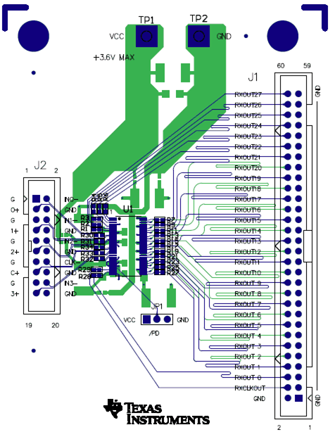
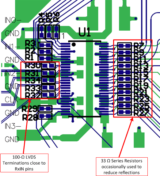
The following images show an example layout of the DS90CR286AT-Q1. Traces in blue correspond to the top layer and the traces in green correspond to the bottom layer. Note that differential pair inputs to the DS90CR286AT-Q1 are tightly coupled and close to the connector pins. In addition, observe that the power supply decoupling capacitors are placed as close as possible to the power supply pins with through vias in order to minimize inductance.
 Figure 29. Example Layout with DS90CR286AT-Q1 (U1).
 Figure 30. Example Layout Close-up.