SNLS013F June 1998 – June 2016 DS90LV028A
PRODUCTION DATA.
- 1 Features
- 2 Applications
- 3 Description
- 4 Revision History
- 5 Pin Configuration and Functions
- 6 Specifications
- 7 Parameter Measurement Information
- 8 Detailed Description
- 9 Application and Implementation
- 10Power Supply Recommendations
- 11Layout
- 12Device and Documentation Support
- 13Mechanical, Packaging, and Orderable Information
Package Options
Mechanical Data (Package|Pins)
Thermal pad, mechanical data (Package|Pins)
Orderable Information
11 Layout
11.1 Layout Guidelines
Use at least 4 PCB board layers (top to bottom): LVDS signals, ground, power, and TTL signals.
Isolate TTL signals from LVDS signals, otherwise the TTL signals may couple onto the LVDS lines. Best practice places TTL and LVDS on different layers which are isolated by a power or ground plane(s).
Keep drivers and receivers as close to the (LVDS port side) connectors as possible.
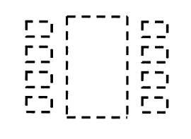
For PC board considerations for the WSON package, please refer to AN-1187, Leadless Leadframe Package (SNOA401). It is important to note that to optimize signal integrity (minimize jitter and noise coupling), the WSON thermal land pad, which is a metal (normally copper) rectangular region placed under the package as seen in Figure 23, must be attached to ground and match the dimensions of the exposed pad on the PCB (1:1 ratio).
11.1.1 Differential Traces
Use controlled impedance traces which match the differential impedance of your transmission medium (that is, cable) and termination resistor. Run the differential pair trace lines as close together as possible as soon as they leave the IC (stubs must be <10 mm long). This helps eliminate reflections and ensure noise is coupled as common mode. In fact, we have seen that differential signals which are 1mm apart radiate far less noise than traces 3 mm apart because magnetic field cancellation is much better with the closer traces. In addition, noise induced on the differential lines is much more likely to appear as common mode which is rejected by the receiver.
Match electrical lengths between traces to reduce skew. Skew between the signals of a pair means a phase difference between signals which destroys the magnetic field cancellation benefits of differential signals and the EMI result. The velocity of propagation, v = c/E r where c (the speed of light) = 0.2997 mm/ps or 0.0118 in/ps. Do not rely solely on the autoroute function for differential traces. Carefully review dimensions to match differential impedance and provide isolation for the differential lines. Minimize the number of vias and other discontinuities on the line.
Avoid 90° turns (these cause impedance discontinuities). Use arcs or 45° bevels.
Within a pair of traces, the distance between the two traces must be minimized to maintain common mode rejection of the receivers. On the printed-circuit board, this distance must remain constant to avoid discontinuities in differential impedance. Minor violations at connection points are allowable.
11.1.2 Termination
Use a termination resistor which best matches the differential impedance or your transmission line. The resistor must be between 90 Ω and 130 Ω. Remember that the current mode outputs require the termination resistor to generate the differential voltage. LVDS does not work correctly without resistor termination. Typically, connecting a single resistor across the pair at the receiver end will suffice.
Surface mount 1% to 2% resistors are the best. PCB stubs, component lead, and the distance from the termination to the receiver inputs must be minimized. The distance between the termination resistor and the receiver must be <10 mm (12 mm maximum).
11.2 Layout Examples
 Figure 23. WSON Thermal Land Pad and Pin Pads
 Figure 24. Simplified DS90LV027A and DS90LV028A Layout