SNLS011D July 1999 – August 2016 DS90LV032A
PRODUCTION DATA.
- 1 Features
- 2 Applications
- 3 Description
- 4 Revision History
- 5 Pin Configuration and Functions
- 6 Specifications
- 7 Parameter Measurement Information
- 8 Detailed Description
- 9 Application and Implementation
- 10Power Supply Recommendations
- 11Layout
- 12Device and Documentation Support
- 13Mechanical, Packaging, and Orderable Information
Package Options
Mechanical Data (Package|Pins)
Thermal pad, mechanical data (Package|Pins)
Orderable Information
9 Application and Implementation
NOTE
Information in the following applications sections is not part of the TI component specification, and TI does not warrant its accuracy or completeness. TI’s customers are responsible for determining suitability of components for their purposes. Customers should validate and test their design implementation to confirm system functionality.
9.1 Application Information
The DS90LV032A LVDS receiver and DS90LV031A driver are intended to be primarily used in an uncomplicated point-to-point configuration as shown in Figure 8. This configuration provides a clean signaling environment for the fast edge rates of the drivers. The receiver is connected to the driver through a balanced media which may be a standard twisted pair cable, a parallel pair cable, or simply PCB traces. Typically the characteristic impedance of the media is in the range of 100 Ω.
9.1.1 Probing LVDS Transmission Lines
Always use high impedance (>100 kΩ), low capacitance (<2 pF) scope probes with a wide bandwidth (1 GHz) scope. Improper probing gives deceiving results.
9.1.2 Cables and Connectors, General Comments
When choosing cable and connectors for LVDS it is important to remember:
- Use controlled impedance media.
- Balanced cables (that is, twisted pair) are usually better than unbalanced cables (such as ribbon cable or simple coax) for noise reduction and signal quality.
The cables and connectors you use must have a matched differential impedance of about 100 Ω. They must not introduce major impedance discontinuities.
Balanced cables tend to generate less EMI due to field canceling effects and also tend to pick up electromagnetic radiation as common-mode (not differential mode) noise which is rejected by the receiver. For cable distances <0.5 m, most cables can be made to work effectively. For distances 0.5 m ≤ d ≤ 10 m, Category 3 (CAT 3) twisted pair cable works well, is readily available, and relatively inexpensive.
9.2 Typical Application
 Figure 8. Balanced System Point-to-Point Application
9.2.1 Design Requirements
When using LVDS devices, it is important to remember to specify controlled impedance PCB traces, cable assemblies, and connectors. All components of the transmission media must have a matched differential impedance of about 100 Ω. They must not introduce major impedance discontinuities. Balanced cables (for example, twisted pair) are usually better than unbalanced cables (ribbon cable) for noise reduction and signal quality. Balanced cables tend to generate less EMI due to field canceling effects and also tend to pick up electromagnetic radiation as common-mode (not differential mode) noise which is rejected by the LVDS receiver.
For cable distances < 0.5 m, most cables work effectively. For distances 0.5 m ≤ d ≤ 10 m, Category 5 (CAT5) twisted pair cable works well, is readily available, and relatively inexpensive.
9.2.2 Detailed Design Procedure
9.2.2.1 Probing LVDS Transmission Lines
Always use high impedance (>100 kΩ), low capacitance (<2 pF) scope probes with a wide bandwidth (1 GHz) scope. Improper probing gives deceiving results.
9.2.3 Application Curves
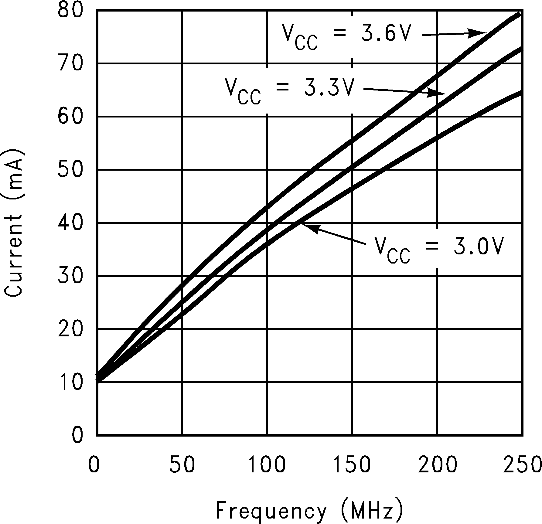
 Figure 9. ICC vs Frequency, Four Channels Switching
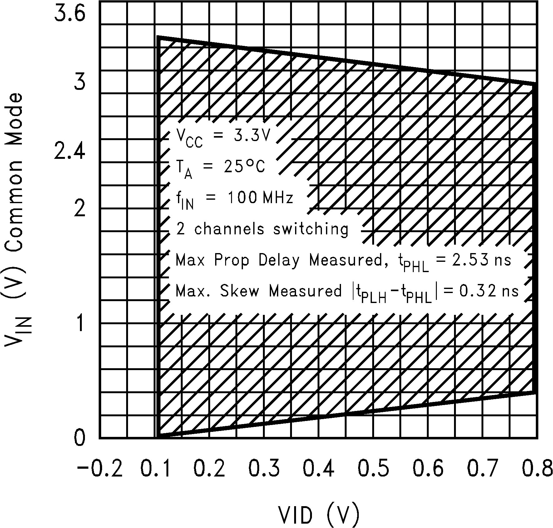
 Figure 10. Typical Common Mode Range Variation
With Respect to Amplitude of Differential Input